Semiconductor integrated circuit device

Inactive Publication Date: 2019-02-14
KEIO UNIV
View PDF1 Cites 0 Cited by
  • Summary
  • Abstract
  • Description
  • Claims
  • Application Information

AI Technical Summary

Benefits of technology

[0017]The disclosed semiconductor integrated circuit device makes it possible to achieve both an improvement in the degree of inductive coup

Problems solved by technology

When there is a metal plate in the vicinity of a coil, however, an inductive current in eddy form (eddy current) is generated within the metal in such a directi

Method used


Image

  • Semiconductor integrated circuit device
  • Semiconductor integrated circuit device
  • Semiconductor integrated circuit device

Examples


example 1

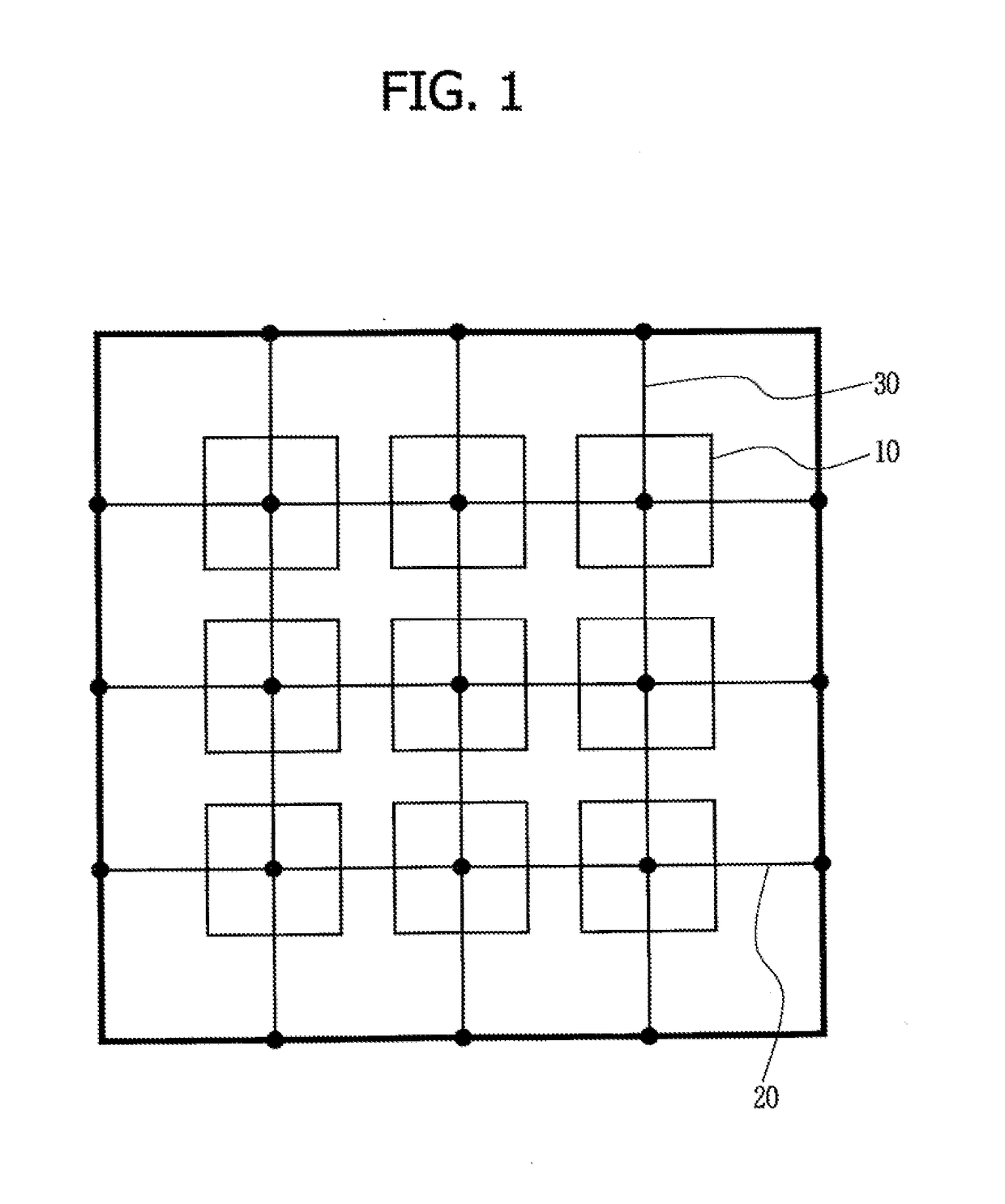
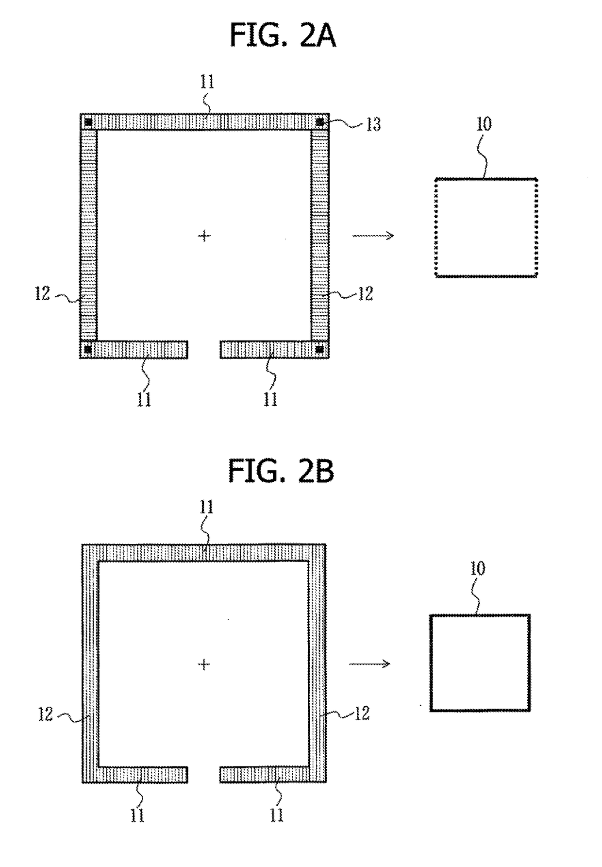
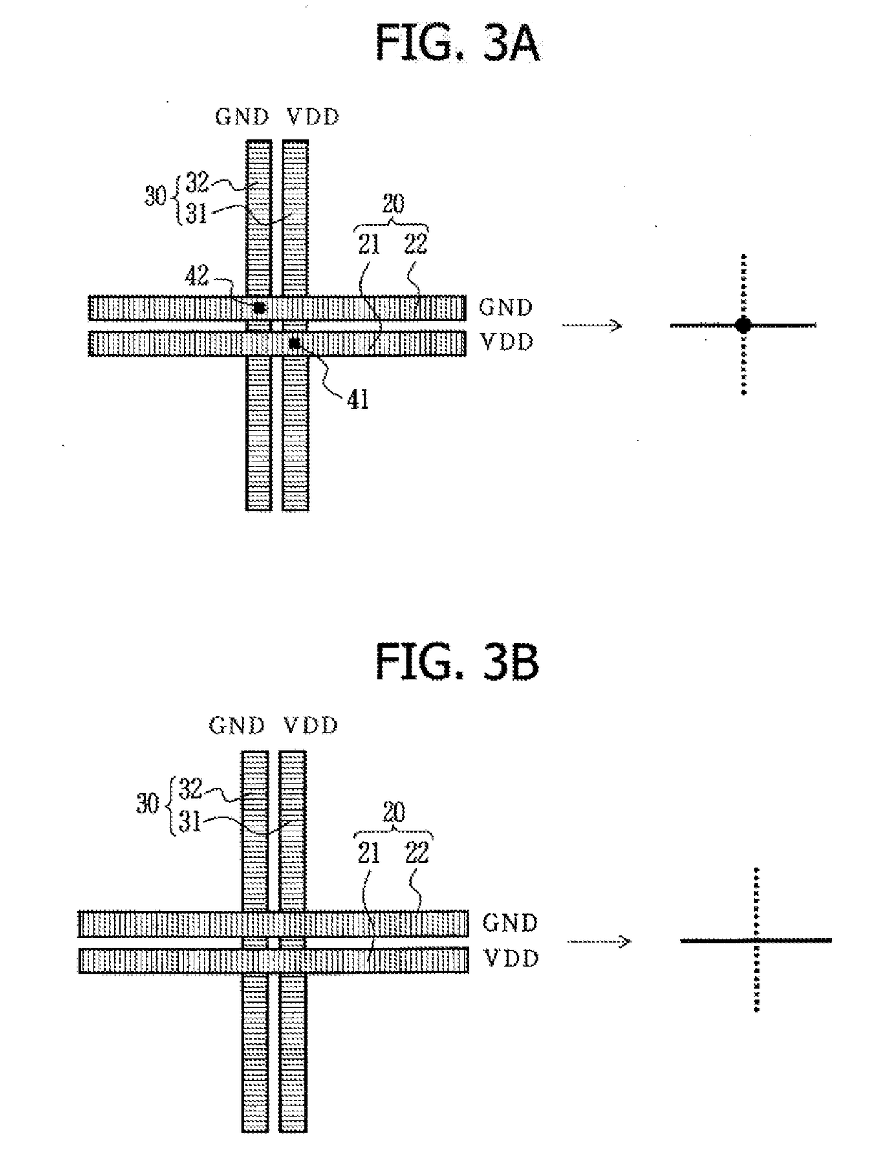
[0064]Next, the semiconductor integrated circuit device according to Example 1 of the present invention is described in reference to FIGS. 9A through 10. FIGS. 9A and 9B are diagrams illustrating the semiconductor integrated circuit device according to Example 1 of the present invention. FIG. 9A is a diagram symbolically illustrating an area where a transmission and reception coil array is arranged, and FIG. 9B is a cross-sectional diagram schematically illustrating the area where a transmission and reception coil array is arranged. As illustrated in FIG. 9A, a power supply wire pair 60 passes through the vicinity of the center of each coil 50 in the X direction, and a power supply wire pair 70 passes through the vicinity of the center of each coil 50 in the Y direction. Power supply wires in the power supply wire pair 60 and in the power supply wire pair 70 are connected to each other through a via 80 in the center portion of each coil 50. In addition, ground wires in the power sup...

example 2

[0069]Next, the semiconductor integrated circuit device according to Example 2 of the present invention is described in reference to FIGS. 11A and 11B. FIGS. 11A and 11B are diagrams illustrating the semiconductor integrated circuit device according to Example 2 of the present invention. FIG. 11A is a diagram symbolically illustrating an area where a transmission and reception coil array is arranged, and FIG. 11B is a cross-sectional diagram schematically illustrating the area where a transmission and reception coil array is arranged. As illustrated in FIG. 11A, power supply wire pairs 60 pass through the vicinity of the center of each coil 90 in the X direction as viewed in the direction in which the layers are layered, power supply wire pairs 70 pass through the vicinity of the center of each coil 90 in the Y direction, the power supply wires of the power supply wire pairs 60 and the power supply wire pairs 70 are connected to each other through vias 80, and the ground wires of th...

example 3

[0072]Next, the semiconductor integrated circuit device according to Example 3 of the present invention is described in reference to FIGS. 12A and 12B. FIGS. 12A and 12B are diagrams illustrating the semiconductor integrated circuit device according to Example 3 of the present invention. FIG. 12A is a diagram symbolically illustrating an area where a transmission and reception coil array is arranged, and FIG. 12B is a cross-sectional diagram schematically illustrating the area where a transmission and reception coil array is arranged. As illustrated in FIG. 12A, power supply wire pairs 60 pass through the vicinity of the center of each coil 90 in the X direction as viewed in the direction in which the layers are layered, power supply wire pairs 70 pass through the vicinity of the center of each coil 90 in the Y direction, the power supply wires of the power supply wire pairs 60 and the power supply wire pairs 70 are connected to each other through vias 80, and the ground wires of th...


PUM


Abstract

The invention relates to a semiconductor integrated circuit device where it is made possible to achieve both an improvement in the degree of inductive coupling between coils and suppression of the power supply voltage drop in the power supply wires. A power supply network is provided with: a first power supply wire group that passes through the inside of every coil of a first coil array formed in the same level in a multilayered wire structure provided on a substrate, in the X direction as viewed in the direction in which the multilayered wire structure is layered, and a second power supply wire group that passes through the inside of every coil in the Y direction, wherein at least part of the first power supply wire group and at least part of the second power supply wire group form a closed circuit that surrounds the periphery of each coil.

Description

TECHNICAL FIELD[0001]The present invention relates to a semiconductor integrated circuit device, and in particular, relates to the configuration of a power supply network that does not prevent inductive coupling in a semiconductor integrated circuit device having transmission and reception coils for data communication using inductive coupling.BACKGROUND ART[0002]A magnetic field passes through a semiconductor chip. When a coil for transmission and a coil for reception that are fabricated by winding a wire on a semiconductor chip are arranged in close proximity and a current that flows through the transmission coil is changed in accordance with a signal, the magnetic field around the coils change together. At this time, a voltage signal is induced in the reception coil, and the signal is decoded via a reception circuit. Such data communication using inductive coupling is used for a digital signal connection between chips that are layered on top of each other.[0003]Data communication ...

Claims


Application Information

Patent Timeline
IPC IPC(8): H01L49/02H01L23/528H01L23/522
CPCH01L28/10H01L23/5286H01L23/5227H01L23/5226H01L21/3205H01L21/768H01L21/822H01L27/04
Inventor KURODA, TADAHIRO
Owner KEIO UNIV
Why Eureka
Try Eureka