Methods for filling a gap feature on a substrate surface and related semiconductor device structures

a technology of semiconductor devices and features, applied in the direction of coatings, basic electric elements, chemical vapor deposition coatings, etc., can solve the problems of increasing difficulty in filling the multitude of gap features with metals having the desired characteristics, and processes commonly do not achieve the desired gap fill capability

Pending Publication Date: 2019-02-28
ASM IP HLDG BV
View PDF4 Cites 263 Cited by
  • Summary
  • Abstract
  • Description
  • Claims
  • Application Information

AI Technical Summary

Benefits of technology

[0009]For purposes of summarizing the invention and the advantages achieved over the prior art, certain objects and advantages of the invention have been described herein above. Of course, it is to be understood that not necessarily all such objects or advantages may be achieved in accordance with any particular embodiment of the invention. Thus, for example, those skilled in the art will recognize that the invention may be embodied or carried out in a manner that achieves or optimizes one advantage or group of advantages as taught or suggested herein without necessarily achieving other objects or advantages as may be taught or suggested herein.

Problems solved by technology

As semiconductor device structure geometries have decreased and high aspect ratio features have become more common place in such semiconductor device structures as DRAM, flash memory, and logic, it has become increasingly difficult to fill the multitude of gap features with a metal having the desired characteristics.
Deposition methods such as high density plasma (HDP), sub-atmospheric chemical vapor deposition (SACVD), and low pressure chemical vapor deposition (LPCVD) have been used for gap fill processes, but these processes commonly do not achieve the desired gap fill capability.

Method used


Image

  • Methods for filling a gap feature on a substrate surface and related semiconductor device structures
  • Methods for filling a gap feature on a substrate surface and related semiconductor device structures
  • Methods for filling a gap feature on a substrate surface and related semiconductor device structures

Examples


Embodiment Construction

[0016]Although certain embodiments and examples are disclosed below, it will be understood by those in the art that the invention extends beyond the specifically disclosed embodiments and / or uses of the invention and obvious modifications and equivalents thereof. Thus, it is intended that the scope of the invention disclosed should not be limited by the particular disclosed embodiments described below.

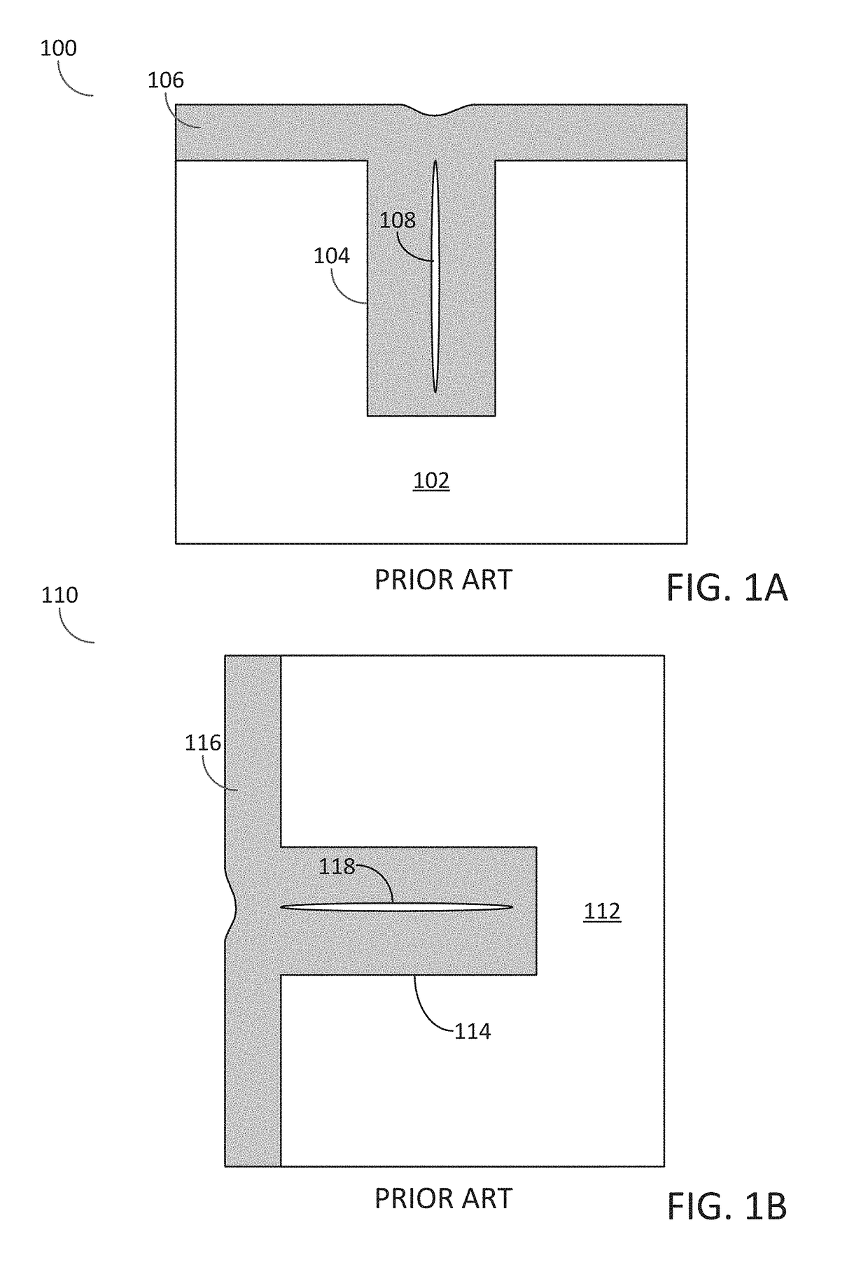
[0017]The illustrations presented herein are not meant to be actual views of any particular material, structure, or device, but are merely idealized representations that are used to describe embodiments of the disclosure.

[0018]As used herein, the term “substrate” may refer to any underlying material or materials that may be used, or upon which, a device, a circuit, or a film may be formed.

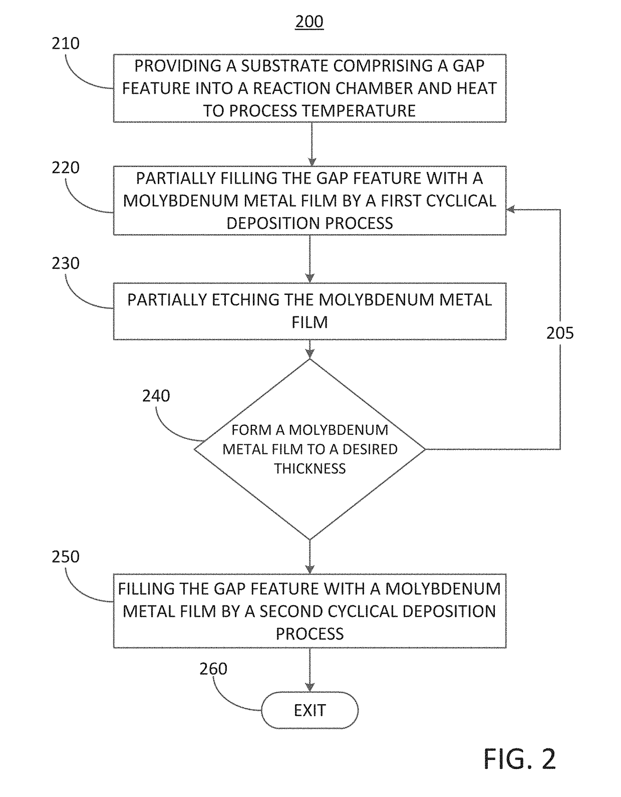
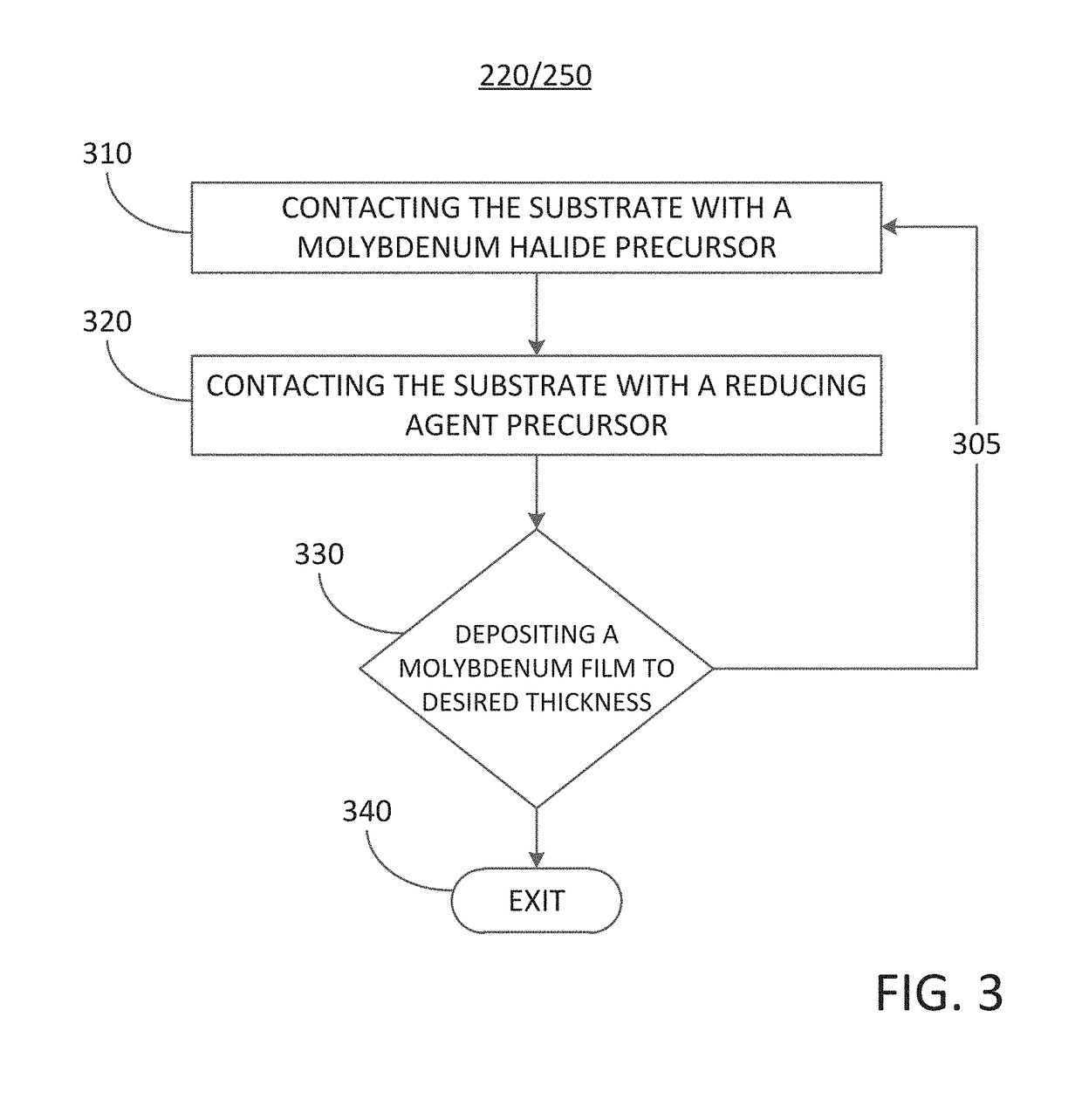
[0019]As used herein, the term “cyclic deposition” may refer to the sequential introduction of one or more precursors (reactants) into a reaction chamber to deposit a film over a substrate and include...


PUM

PropertyMeasurementUnit
temperatureaaaaaaaaaa
pressureaaaaaaaaaa

Abstract

Methods for filling a gap feature on a substrate surface are disclosure. The methods may include: providing a substrate comprising one or more gap features into a reaction chamber; and partially filling the one or more gap features with a molybdenum metal film by a cyclical deposition-etch process, wherein a unit cycle of the cyclical deposition-etch process comprises: partially filling the one or more gap features with a molybdenum metal film by a performing at least one unit cycle of a first cyclical deposition process; and partially etching the molybdenum metal film. The methods may also include: filling the one or more gap features with molybdenum metal film by performing at least one unit cycle of a second cyclical deposition process. Semiconductor device structures including a gap fill molybdenum metal film disposed in one or more gap features in or on a surface of a substrate formed by the methods of the disclosure are also disclosed.

Description

CROSS-REFERENCE TO RELATED APPLICATION[0001]The present application claims priority to: U.S. Non-Provisional patent application Ser. No. 15 / 691,241, entitled “Layer Forming Method” and filed on Aug. 30, 2017; U.S. Provisional Patent Application No. 62 / 607,070, entitled “Layer Forming Method” and filed on Dec. 18, 2017; and U.S. Provisional Patent Application No. 62 / 619,579, entitled “Deposition Method” and filed on Jan. 19, 2018.FIELD OF INVENTION[0002]The present disclosure relates generally to methods for filling a gap feature on a substrate surface and particularly methods for filling one or more gap features with a molybdenum metal film utilizing a cyclical deposition-etch process. The present disclosure also generally relates to semiconductor device structures including one or more gap features filled with a molybdenum metal film.BACKGROUND OF THE DISCLOSURE[0003]Semiconductor fabrication processes for forming semiconductor device structures, such as, for example, transistors, ...

Claims


Application Information

Patent Timeline
Patent Type & Authority Applications(United States)
IPC IPC(8): H01L21/285H01L21/3213H01L23/532C23C16/14C23C16/455
CPCC23C16/45553H01L23/53257H01L21/28568H01L21/32135H01L21/28556C23C16/14C23C16/045C23C16/56C23C16/45523C23C16/45525H01L21/76877H01L21/28562H01L21/76876H01L21/0228H01L21/76828H01L21/02205H01L2924/01042
Inventor SHRESTHA, KIRANZOPE, BHUSHANSWAMINATHAN, SHANKARZHU, CHIYUJUSSILA, HENRI TUOMAS ANTEROXIE, QI
Owner ASM IP HLDG BV
Why Eureka
Try Eureka