Multi-blade and processing method of workpiece

Active Publication Date: 2019-02-28
DISCO CORP
View PDF0 Cites 2 Cited by
  • Summary
  • Abstract
  • Description
  • Claims
  • Application Information

AI Technical Summary

Benefits of technology

The present invention provides a multi-blade that can give inclinations or steps to chip side surfaces simultaneously with dividing into individual chips and a processing method of a workpiece using the multi-blade. The multi-blade simultaneously cuts the workpiece along the planned dividing lines and divides it into chips. The outer surface of the spacer between the cutting blades is covered by the abrasive grain layer, which grinds the workpiece and transfers the outer surface shape of the spacer to the chip. This results in various shapes being given to the outer surfaces of the chips simultaneously with the dividing, reducing workman-hours and shortening the processing time.

Problems solved by technology

However, the substrate needs to be cut in a stepwise manner by using two kinds of blades and there is a problem that the work man-hours increase and the work time becomes longer.

Method used


Image

  • Multi-blade and processing method of workpiece
  • Multi-blade and processing method of workpiece
  • Multi-blade and processing method of workpiece

Examples


Embodiment Construction

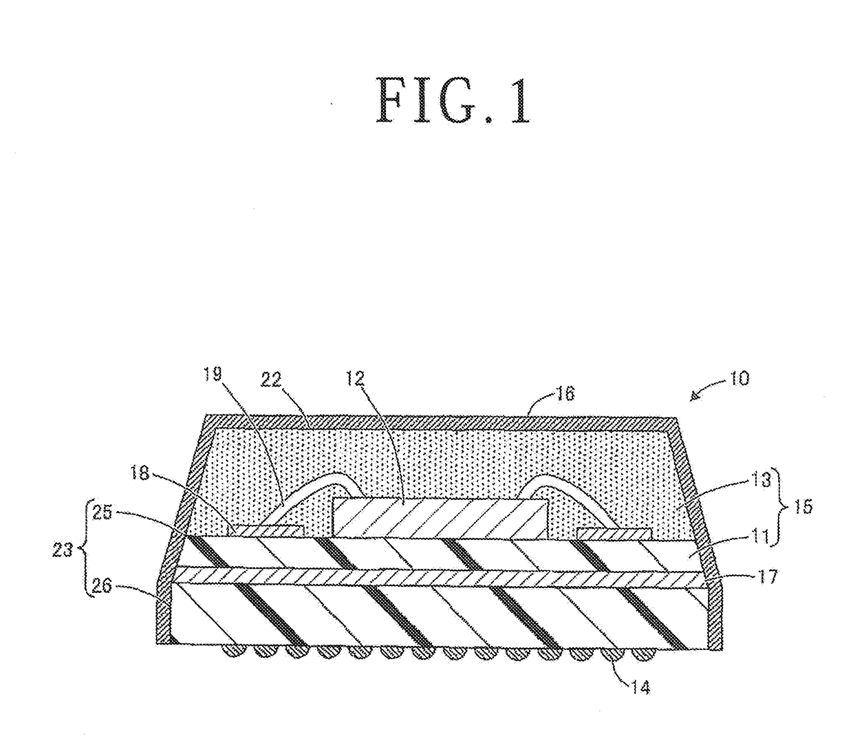
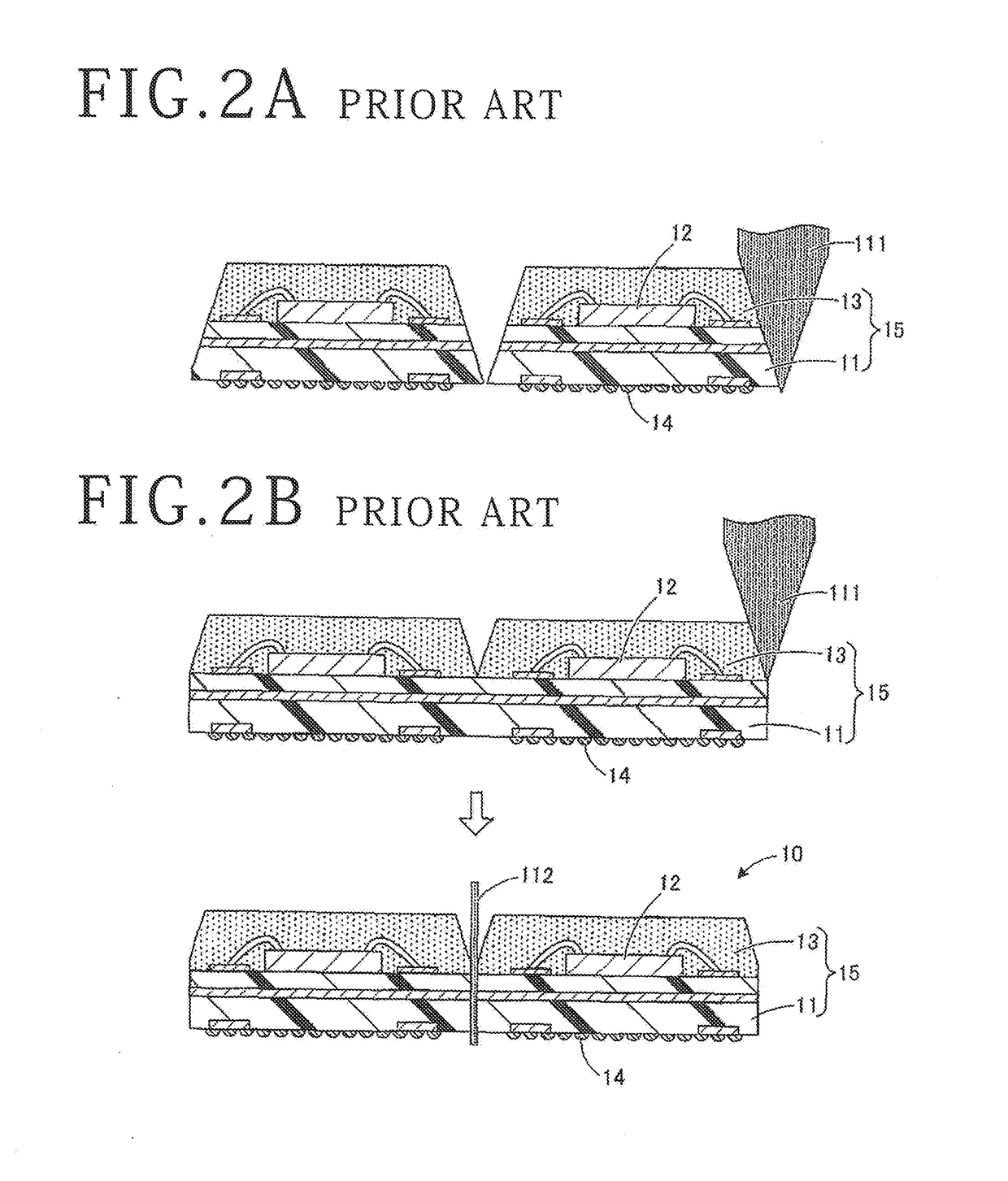
[0024]A processing method of the present embodiment will be described below with reference to the accompanying drawings. In the following description, explanation will be made with exemplification of a package substrate as a substrate. However, the kind of substrate is not limited to the package substrate. FIG. 1 is a sectional schematic diagram of a semiconductor package of the present embodiment. FIG. 2A and FIG. 2B are sectional schematic diagrams depicting manufacturing methods of a semiconductor package in comparative examples. The following embodiment merely depicts one example and another step may be included between the respective steps and the order of steps may be changed as appropriate.

[0025]As depicted in FIG. 1, a semiconductor package 10 is semiconductor apparatus of all packages that need blocking due to so-called electro-magnetic interference (EMI) and is configured to suppress leakage of electromagnetic noise to the surroundings by a shield layer 16 of the outer sur...


PUM


Abstract

A multi blade that processes semiconductor packages into a desired shape while dividing a package substrate includes plural cutting blades that divide the package substrate into the individual semiconductor packages and a spacer provided between two cutting blades adjacent to each other, and is configured in such a manner that the cutting blades and the spacer have the same rotation axis center. The outer surface of the spacer is formed into a transfer shape of the semiconductor package and is covered by an abrasive grain layer, and the upper surface of the package substrate is ground by the outer surface of the spacer simultaneously with cutting of the package substrate by the plural cutting blades.

Description

BACKGROUND OF THE INVENTIONField of the Invention[0001]The present invention relates to a multi-blade and a processing method of a workpiece.Description of the Related Art[0002]In a device manufacturing step, individual device chips are formed by cutting various kinds of substrates such as a wafer and a semiconductor package substrate by a cutting blade along streets. As such a processing method, a step cut is known by which the cutting depth is increased in a stepwise manner with respect to a substrate by using two kinds of blades. In the step cut, a shallow groove of a first step is formed along a street of a substrate by a large-width straight blade or V-blade. Then, the bottom surface of the shallow groove is deeply cut by a small-width straight blade and the substrate is fully cut (for example, refer to Japanese Patent Laid-open No. 2015-018965).SUMMARY OF THE INVENTION[0003]Incidentally, depending on the kind of substrate, there is a demand for giving various shapes such as in...

Claims


Application Information

Patent Timeline
IPC IPC(8): H01L21/67H01L21/78H01L21/56H01L21/48H01L23/00H01L23/31H01L23/498H01L23/552B24D5/12
CPCH01L21/67092H01L21/78H01L21/561H01L21/4853H01L24/48H01L23/3114H01L23/49811H01L23/49838H01L23/552B24D5/123H01L2224/48227H01L2924/3025H01L2924/181H01L23/3128H01L21/565H01L2924/00014H01L2224/48229H01L2924/00012H01L2224/45099
Inventor JANG, BYEONGDECKKIM, YOUNGSUKISHII, TAKAHIROSAKAI, MAKI
Owner DISCO CORP
Why Eureka
Try Eureka