Light-emitting device, light source unit, and projection display apparatus
- Summary
- Abstract
- Description
- Claims
- Application Information
AI Technical Summary
Benefits of technology
Problems solved by technology
Method used
Image


Examples
first embodiment
1. FIRST EMBODIMENT
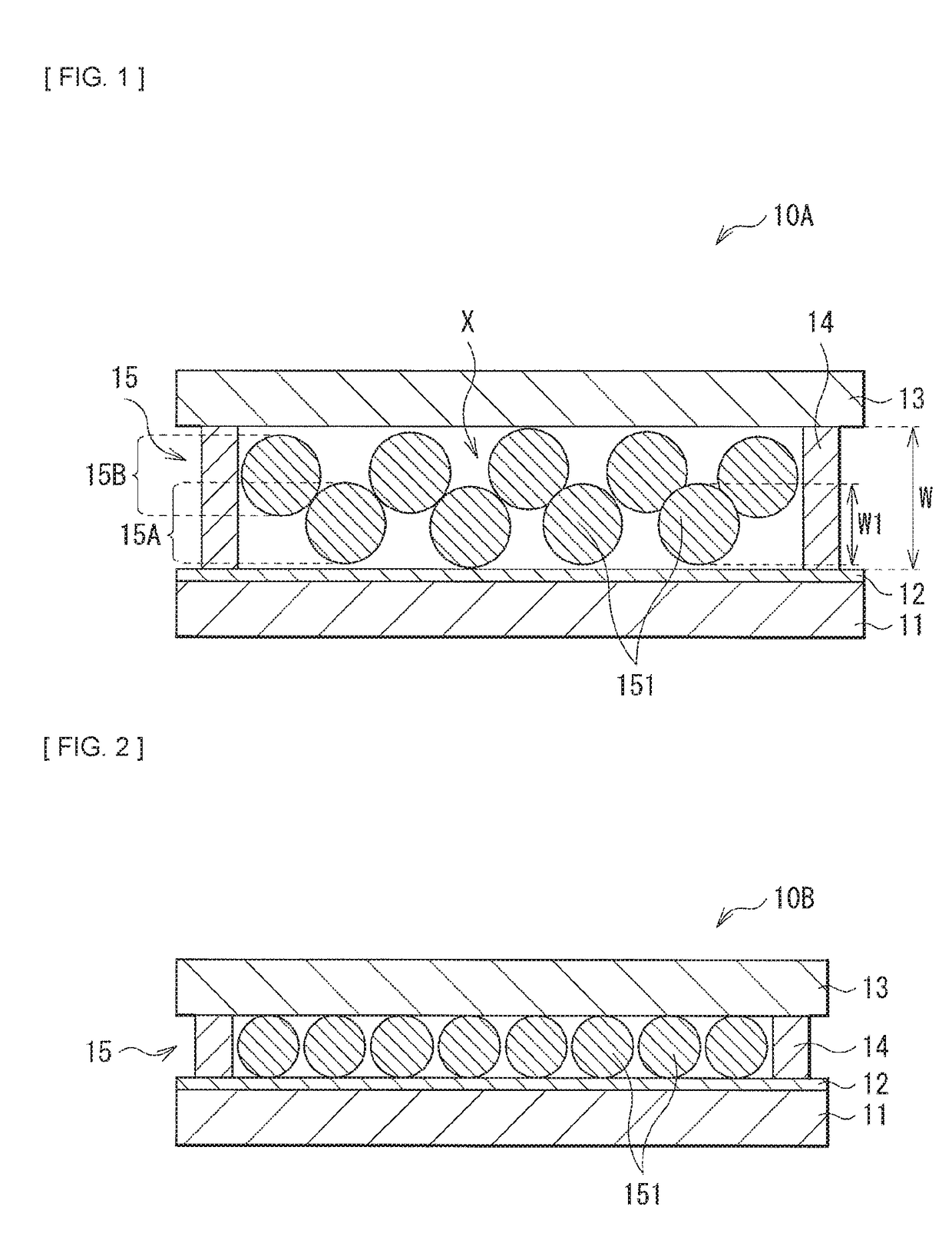
[0039]FIG. 1 illustrates a cross-sectional configuration of a light-emitting device (light-emitting device 10A) according to a first embodiment of the present disclosure. The light-emitting device 10A is also referred to as a phosphor wheel (phosphor wheel 10). The light-emitting device 10A is used as, for example, a light-emitting device that configures a light source optical system (for example, light source unit 1) of a later-described projection display apparatus (projector 100) (for example, refer to FIGS. 4 and 11). The light-emitting device 10A of the present embodiment is configured such that a part between bases including a pair of thin plates (a supporting base 11 and a sealing base 13) is filled with a plurality of phosphor particles 151. The pair of thin plate bases has, for example, a circular planar shape, and is disposed to face each other with a predetermined space being provided. It is to be noted that FIGS. 1, 3A, and 3B schematically illustrate ...
second embodiment
2. SECOND EMBODIMENT
[0062]FIG. 5 illustrates a cross-sectional configuration of a light-emitting device (light-emitting device 20A) according to the second embodiment of the present disclosure. Similarly to the above-described first embodiment, in the light-emitting device 20A, a phosphor layer 25 having phosphor particles 251 is provided between the supporting base 11 and the sealing base 13. The present embodiment includes a configuration in which surfaces of the phosphor particles 251 are each covered by an optical thin film 252. It is to be noted that FIG. 5 schematically illustrates a configuration of the light-emitting device 20A, and may differ from an actual dimension or shape thereof.
[0063]The optical thin film 252 includes, for example, a plurality of dielectric films having different refractive indices to each other, in a stacked manner. Examples of a material that configures the optical thin film 252 include inorganic dielectric materials such as a silicic acid compound,...
modification example 1
3. MODIFICATION EXAMPLE 1
[0065]FIG. 6 illustrates a cross-sectional configuration of a light-emitting device (light-emitting device 20B) as a modification example according to the above-described second embodiment. Similarly to the above-described first embodiment, in the light-emitting device 20B, the phosphor layer 25 including the phosphor particles 251 is provided between the supporting base 11 and the sealing base 13. The present modification example includes a configuration in which surfaces of the phosphor particles 251 are each covered by a crosslinking film 253. It is to be noted that FIG. 6 schematically illustrates a configuration of the light-emitting device 20B, and may differ from an actual dimension or shape thereof.
[0066]The crosslinking film 253 includes, for example, glass that is synthesized with orthosilicic acid tetraalkyl (such as orthosilicic acid tetramethyl (TMOS) and orthosilicic acid tetraethyl (TEOS)) or waterglass (sodium silicate or silicic acidpotassiu...
PUM
| Property | Measurement | Unit |
|---|---|---|
| Current | aaaaa | aaaaa |
| Porosity | aaaaa | aaaaa |
| Porosity | aaaaa | aaaaa |
Abstract
Description
Claims
Application Information