Photo-detection device, imaging apparatus, and imaging system

a technology of image detection device and imaging apparatus, which is applied in the direction of radiation controlled devices, instruments, optical radiation measurement, etc., can solve the problems of abnormal operation of the other element, the potential of the other element or the bias potential of the other photo-detection device that shares the same dc bias power source, and the effect of affecting the other elemen

Active Publication Date: 2019-04-18
CANON KK
View PDF0 Cites 33 Cited by
  • Summary
  • Abstract
  • Description
  • Claims
  • Application Information

AI Technical Summary

Benefits of technology

[0004]In a photo-detection device including an avalanche photodiode and sharing a power source with another element or another photo-detection device, an effect of a bias change due to a quench action performed by the photo-detection device on the other element or the other photo-detection device can be reduced or avoided.

Problems solved by technology

In this case, when the quench signal is fed back to the DC bias in a photo-detection device, the potential at the other element or the bias potential at the other photo-detection device that shares the same DC bias power source is also affected and therefore changes.
There is therefore a possibility of abnormal operation of the other element, a change in the result of the photo-detection, or no photo-detection.

Method used


Image

  • Photo-detection device, imaging apparatus, and imaging system
  • Photo-detection device, imaging apparatus, and imaging system
  • Photo-detection device, imaging apparatus, and imaging system

Examples


first embodiment

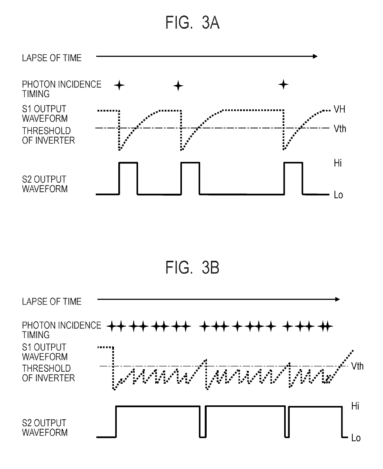
[0018]A photo-detection device in the present embodiment will be described with reference from FIG. 1 to FIGS. 3A and 3B.

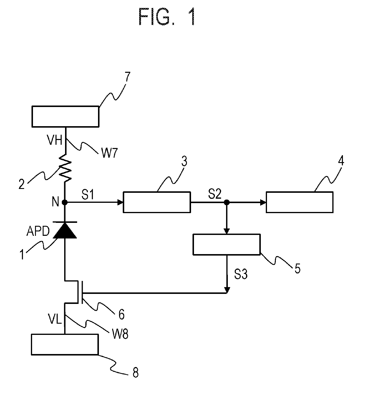
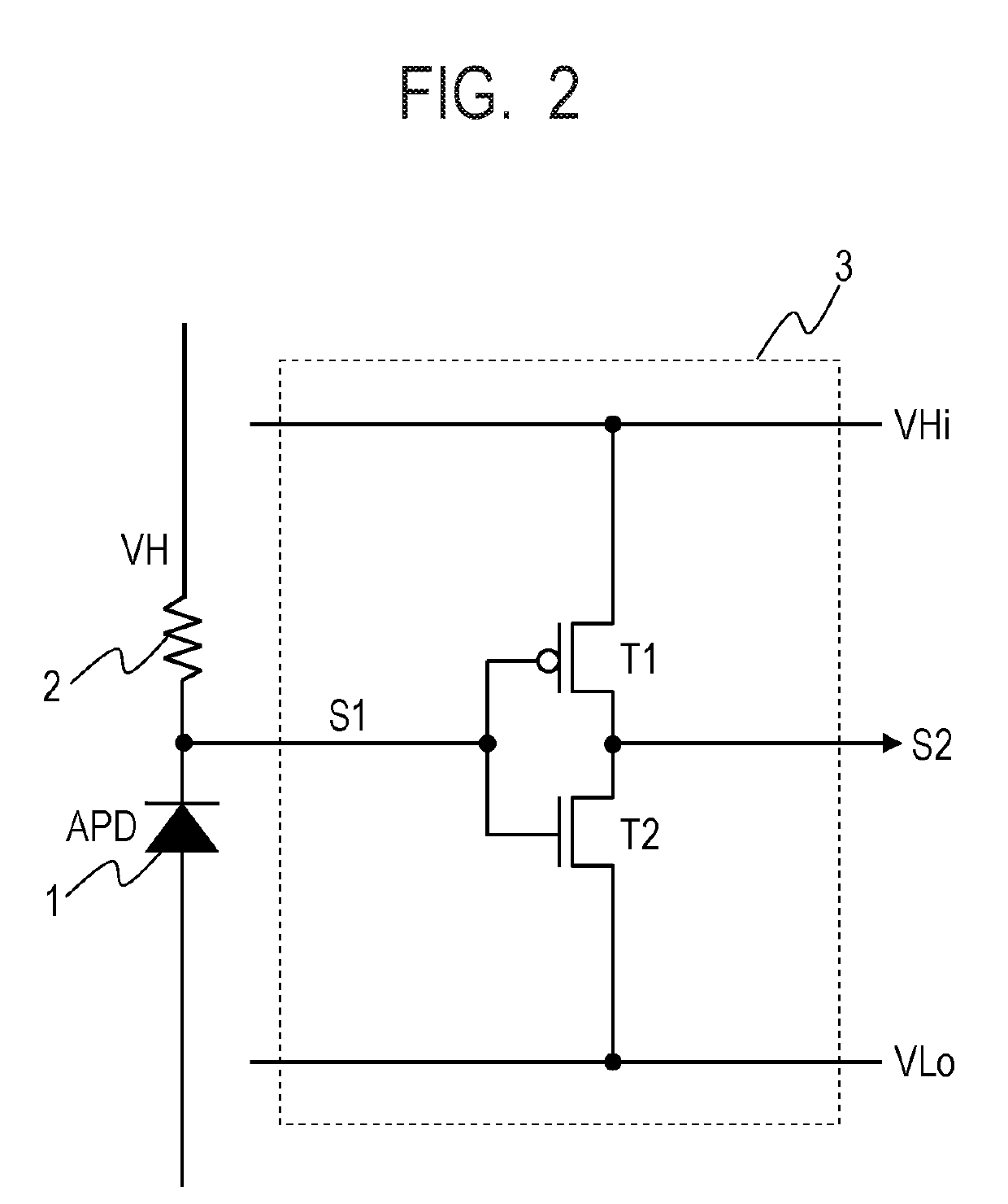
[0019]FIG. 1 is a block diagram illustrating the configuration of the photo-detection device according to the present embodiment, and the photo-detection device includes an avalanche photodiode (hereinafter referred to as APD 1), a resistor element 2, which is a load element, a current detecting unit 3, a counter circuit 4, a quench signal generating unit 5, and a switch. The switch is a quench signal feedback switch, and can, for example, be a transistor 6, such as a MOS transistor.

[0020]In FIG. 1, a voltage signal S1, which is an output from a first terminal of the APD 1, is input to the current detecting unit 3. The resistor element 2, which is a load element, is connected to a node N between the APD 1 and the current detecting unit 3. A signal from the current detecting unit 3 is input to the quench signal generating unit 5, and the quench signal generating un...

second embodiment

[0080]An example of an imaging apparatus will be descried with reference to FIGS. 9 and 10. In the present embodiment, the same configurations, materials, effects, functions, drive method, and other factors as those in the first embodiment will not be described except part thereof.

[0081]FIG. 9 is a block diagram of an imaging apparatus 200 having a plurality of photo-detection devices. The APD 1, which forms each pixel, the variety of elements for signal processing, the method for feeding back the quench signal, and other factors are the same as those in the first embodiment, therefore have the same reference characters, and will not be described in detail, as described above.

[0082]The imaging apparatus 200 includes a pixel unit 106, a control pulse generating unit 109, a horizontal scan circuit unit 104, column circuits 105, signal lines 107, a vertical scan circuit unit 103, and a power source circuit unit 110. A plurality of pixels 100 is arranged in a matrix in the pixel unit 10...

third embodiment

[0096]In the present embodiment, an imaging system using the imaging apparatus 200 according to the second embodiment including the photo-detection device according to the first embodiment will be described with reference to FIG. 11. The same configurations, effects, materials, functions, and methods as those illustrated in FIGS. 1, 9 and 10 have the same reference characters and will not be described in detail.

[0097]FIG. 11 is a block diagram for describing the configuration of an imaging system 300. In FIG. 11, the imaging apparatus 200 is disposed with respect to a light incident surface via a diaphragm mechanism 301, an imaging lens 302, a mirror unit 303, and a mechanical shutter 304.

[0098]The mirror unit 303 is a mirror that moves upward and downward in accordance with an instruction from a system controlling unit 305 in light exposure, a live-view imaging, and motion image capturing to switch the destination of an introduced light flux incident through the imaging lens 302 be...


PUM


Abstract

A photo-detection device includes an APD, a current detecting unit to which a signal via a first terminal of the APD is input, a load element connected to a node between the APD and the current detecting unit, a quench signal generating unit to which a signal from the current detecting unit is input and which outputs a quench signal, and a switch connected to a second terminal of the APD and a first wiring line to which first potential is supplied. The node is connected via the load element to a second wiring line to which second potential different from the first potential is supplied, and the quench signal generating unit generates a one-shot pulse signal as the quench signal based on the signal from the current detecting unit and causes the quench signal to be input to the switch.

Description

BACKGROUND OF THE INVENTIONField of the Invention[0001]An aspect of the present invention relates to a photo-detection device that performs photoelectric conversion, an imaging apparatus, or an imaging system.Description of the Related Art[0002]There has been a known photo-detection device using an avalanche photodiode having an active-quenching mechanism that forcibly stops avalanche current. Japanese Patent Application Laid-Open No. 2006-179587 discloses a photo-detection device that evaluates whether or not avalanche current has occurred and feeds back a quench signal output from quench signal generation unit to the avalanche photodiode when the avalanche current has occurred to perform quenching at high speed.SUMMARY OF THE INVENTION[0003]In the photo-detection device described in Japanese Patent Application Laid-Open No. 2006-179587, the quench signal is superimposed on a DC bias and the resultant bias is applied to the cathode. The photo-detection device shares a DC bias power...

Claims


Application Information

Patent Timeline
Patent Type & Authority Applications(United States)
IPC IPC(8): G01J1/44H01L31/107H01L27/146
CPCG01J1/44H01L31/107H01L27/14636H01L27/14643H01L27/14612G01J2001/442G01J2001/4466G01J2001/4406H04N5/376G01R31/2632H04N25/772H04N25/74
Inventor FUKUCHI, YUSUKE
Owner CANON KK
Why Eureka
Try Eureka