Cutting device for thin semiconductor wafer and cutting method thereof

Active Publication Date: 2019-05-02
ASTI GLOBAL INC
View PDF0 Cites 3 Cited by
  • Summary
  • Abstract
  • Description
  • Claims
  • Application Information

AI Technical Summary

Benefits of technology

[0009]Therefore, through the technical features including “a laser light generator for providing femtosecond laser light having a pulse width on the order of fs,”“a polygonal mirror structure having a plurality of reflective surfaces for reflecting the femtosecond laser light provided by the generator,” and “the polygonal mirror structure rotating continuously with respect to the femtosecond laser light, so that the femtosecond laser light is sequentially and repeatedly reflected by the plurality of reflective surfaces of the polygonal mirror structure and projected on the semicondu

Problems solved by technology

While such metal cutting blades can cut semiconductor materials such as gallium arsenide and silicon carbide, in order to prevent the blades from damaging the cutting surface, the speed that the blades are fed must be controlled to be within a certain range, so that it is difficult to increase production efficiency.
However, traditional galvanometer (Galvo) scanners have reached the limit of 15 m/s in scanning speed, and can

Method used


Image

  • Cutting device for thin semiconductor wafer and cutting method thereof
  • Cutting device for thin semiconductor wafer and cutting method thereof
  • Cutting device for thin semiconductor wafer and cutting method thereof

Examples


Example

First Embodiment

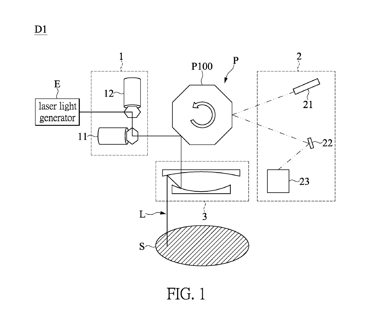
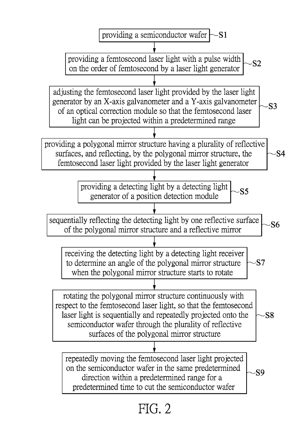
[0020]Reference is made to FIG. 1, which illustrates a cutting device for a thin semiconductor wafer according to the first embodiment of the present disclosure. The present disclosure provides a cutting device D1 for a thin semiconductor wafer, which includes a laser light generator E and a polygonal mirror structure P. In addition, in the present embodiment, the cutting device D1 further includes an optical correction module 1 and a position detection module 2.

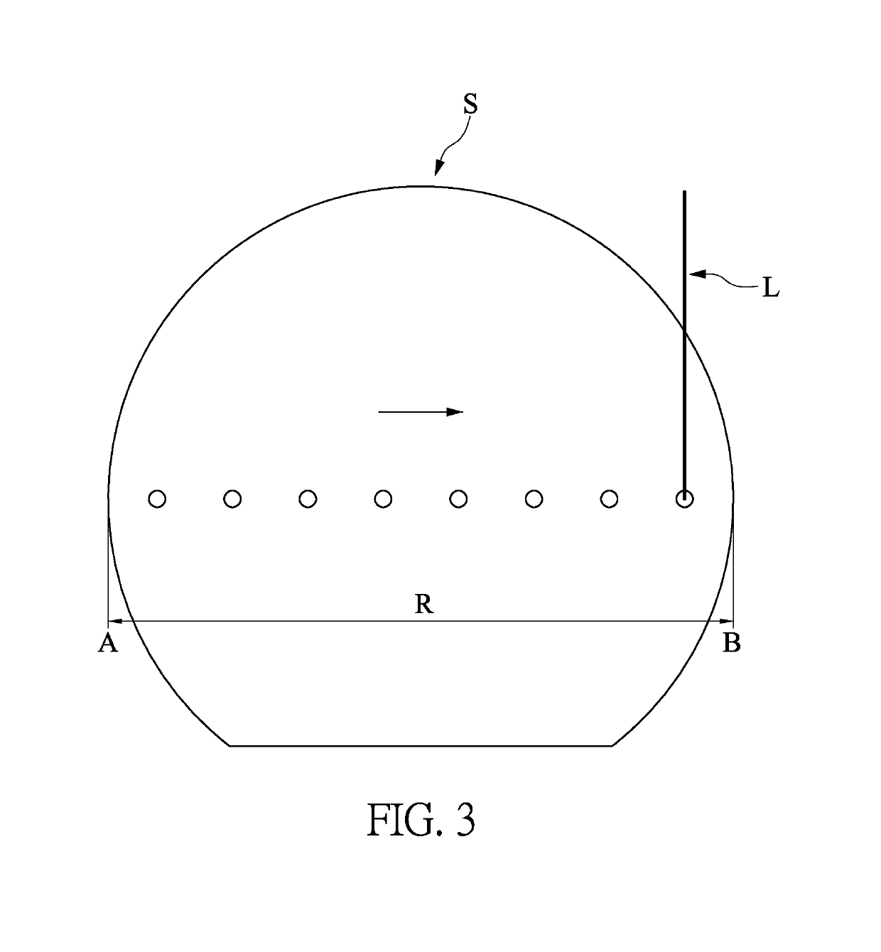
[0021]Specifically, the laser light generator E is used to provide ultrashort pulse light, and the laser light generator E includes an oscillator, a pulse picker, an optical amplifier, and a modulator. In this embodiment, the laser generator E can provide a femtosecond laser light L with a pulse width on the order of fs, and exemplarily less than 500 fs, and the pulse repetition frequency of the femtosecond laser light L can be greater than 1 MHz so as to maintain a small HAZ, which effectively improves the p...

Example

Second Embodiment

[0040]The present disclosure further provides another embodiment. Reference is made to FIG. 9, which illustrates another cutting device D2 for a thin semiconductor wafer according to the second embodiment of the present disclosure. Similar to the first embodiment of the present disclosure, the cutting device D2 includes a laser light generator E, a polygonal mirror structure P, an optical correction module 1 and a position detection module 2. The cutting device D2 further includes a laser beam expander N disposed between the laser light generator E and the optical correction module 1 for adjusting the diameter of the light beam.

[0041]Therefore, through the technical features including “a laser light generator E for providing femtosecond laser light L having a pulse width on the order of fs,”“a polygonal mirror structure P having a plurality of reflective surfaces P100 for reflecting the femtosecond laser light L provided by the generator E” and “the polygonal mirror...


PUM

PropertyMeasurementUnit
Timeaaaaaaaaaa
Thicknessaaaaaaaaaa
Timeaaaaaaaaaa

Abstract

A cutting device for a thin semiconductor wafer includes a laser light generator and a polygonal mirror structure. The laser light generator is used to provide a femtosecond laser light with a pulse width on a femtosecond order (10−15 second). The polygonal mirror structure is used to reflect the femtosecond laser light. The polygonal mirror structure has a plurality of reflective surfaces. The polygonal mirror structure rotates continuously with respect to the femtosecond laser light, such that the femtosecond laser light is sequentially and repeatedly reflected by the plurality of reflective surfaces and projected on a semiconductor wafer. The femtosecond laser light projected on a semiconductor wafer moves repeatedly along a same predetermined direction in a predetermined range during a predetermined time to groove or cut the semiconductor wafer.

Description

CROSS-REFERENCE TO RELATED PATENT APPLICATION[0001]This application claims the benefit of priority to Taiwan Patent Application No. 106137782, filed on Nov. 1, 2017. The entire content of the above identified application is incorporated herein by reference.[0002]Some references, which may include patents, patent applications and various publications, may be cited and discussed in the description of this disclosure. The citation and / or discussion of such references is provided merely to clarify the description of the present disclosure and is not an admission that any such reference is “prior art” to the present disclosure described herein. All references cited and discussed in this specification are incorporated herein by reference in their entireties and to the same extent as if each reference was individually incorporated by reference.FIELD OF THE PRESENT DISCLOSURE[0003]The present disclosure relates to a processing device for a thin semiconductor wafer and method thereof, and mo...

Claims


Application Information

Patent Timeline
IPC IPC(8): B23K26/0622B23K26/03
CPCB23K26/0624B23K26/032B23K2101/40H01L21/67092B23K26/16B23K26/082B23K26/0821B23K26/142B23K26/707
Inventor LIAO, CHIEN-SHOUYU, CHIH-WEI
Owner ASTI GLOBAL INC
Why Eureka
Try Eureka