

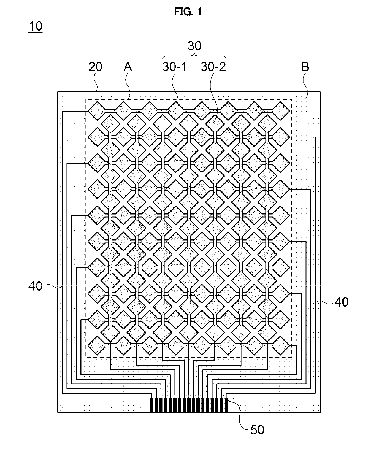
Electrode connection structure and electronic device including the same
a technology of electronic devices and connection structures, applied in the direction of insulated conductors, power cables, cables, etc., can solve the problems of failure to provide solutions for overcoming and cracks in pads, and achieve the effects of improving flexibility properties, enhancing product reliability, and improving adhesion between elements
- Summary
- Abstract
- Description
- Claims
- Application Information
AI Technical Summary
Benefits of technology
Problems solved by technology
Method used
Image

Examples
example 2
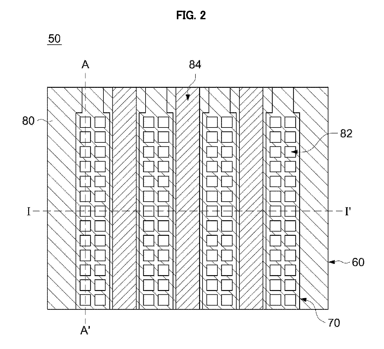
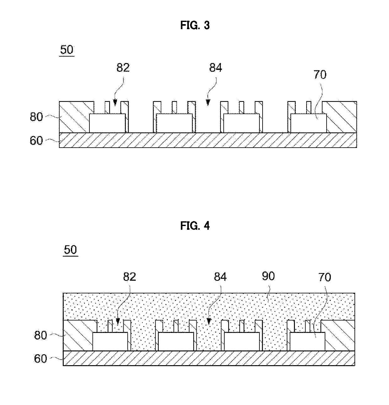
[0106]Processes the same as those of Example 1 were performed except that a second groove line having a width of 10 μm and extending from one end to the other end of the pad was additionally formed as illustrated in FIG. 7 to connect the holes to obtain an electrode connection structure of Example 2.
example 3
[0107]Processes the same as those of Example 2 were performed except that a third groove line having a width of 30 μm was additionally formed to connect the first groove line and the second groove line as illustrated in FIG. 8 to obtain an electrode connection structure of Example 3.
example 4
[0108]Processes the same as those of Example 1 were performed except that a width of the first groove line was periodically changed between 30 μm and 80 μm, and a width of a terminal of the pad on an end portion of the substrate layer was 30 μm as illustrated in FIG. 5 to obtain an electrode connection structure of Example 4.
PUM
 Abstract
Description
Claims
Application Information