Method for Semiconductor Leadframes in Low Volume and Rapid Turnaround

a leadframe and low-volume technology, applied in semiconductor devices, semiconductor/solid-state device details, electrical equipment, etc., can solve the problems of affecting the reliability of devices, wasting time and investment money, and presently taking too much cycle time and investment money to tool up stamping machines, photomasks, etching baths, etc., to achieve strong adhesion between leadframe and polymeric encapsulation, reduce cycle time, and easy to oxidize

Active Publication Date: 2010-11-25
TEXAS INSTR INC
View PDF16 Cites 34 Cited by
  • Summary
  • Abstract
  • Description
  • Claims
  • Application Information

AI Technical Summary

Benefits of technology

[0010]Applicant solved the leadframe manufacturing problems of flexibility, turn-around time, spacing rules, and cost by changing the leadframe production steps from the conventional sequence: first cutting, then plating, to the new sequence: first plating, then cutting, and by simultaneously replacing the conventional fixed cutting tools (stamper, mask) with programmable methods (laser jet, water jet, electrical discharge machining). These computer-controlled techniques also improve the design rules for spacings and widths, creating denser interconnections for improved electrical functionality.
[0012]Applicant discovered that the adhesion between leadframe and polymeric encapsulation can be strongly improved when the sidewalls of leadframe pad and segments have a surface configuration (roughness, metal oxides) with strong intermolecular affinity to polymeric compounds, independent of any plated metal layer on other leadframe surfaces.
[0013]Applicant solved the delamination problem of leadframe and polymeric compound concurrently with the leadframe manufacturing problem by the same change in leadframe production steps, namely first plating, then cutting. In the new leadframe manufacturing flow, a strip of a first metal (e.g., copper) is plated on both surfaces with a layer of a second metal (e.g., nickel). Then, the strip is cut with software-driven equipment (e.g., laser jet), whereby the first metal becomes exposed at the sidewalls of the cuts, and is readily oxidized. In addition, the machining is employed to remove the plated second metal from pre-selected leadframe surface areas (e.g., peripheral pad areas), creating and roughening additional zones (e.g., of copper oxide) for leadframe-to-package adhesion.
[0014]As further benefits, the leadframe fabrication flow of the invention reduces the cycle time for developing new leadframes and introducing new products and any needed initial investment. In addition, the new fabrication flow supports rapid prototyping and designing of experiments, which require multiple variations. Since the computer-numerical controlled tools offer an opportunity to remove certain additional portions of the plated second metal, special features and shapes can be created such as mold locks, mold flow controls, stress-relieving shapes, space for fitting external components, and precision shapes for electrical control.

Problems solved by technology

Applicant recognized that the current semiconductor leadframe manufacturing flow is directed for supporting high-volume products, but is not a good fit for the Analog type businesses, where more than 70% of products do not ramp up to high volumes.
For Analog products, it takes presently too much cycle time and investment money to tool up the stamping machines, photomasks, and etching baths for producing the leadframes.
Furthermore, applicant recognized that the ongoing miniaturization of the device packages enhances the risk of delamination between leadframe and polymeric package and endangers device reliability.
In addition, technical constraints, such as the spacing rules in the leadframe designs, are becoming increasingly restrictive, and the current leadframe fabrication flow cannot support effectively rapid prototyping.

Method used


Image

  • Method for Semiconductor Leadframes in Low Volume and Rapid Turnaround
  • Method for Semiconductor Leadframes in Low Volume and Rapid Turnaround
  • Method for Semiconductor Leadframes in Low Volume and Rapid Turnaround

Examples


Embodiment Construction

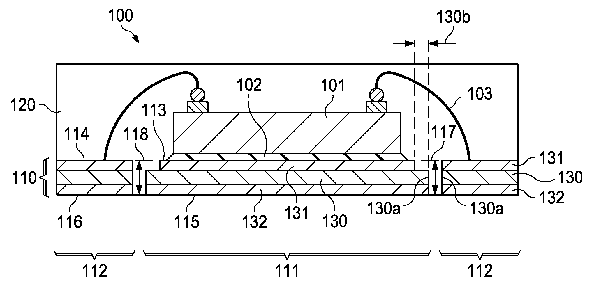
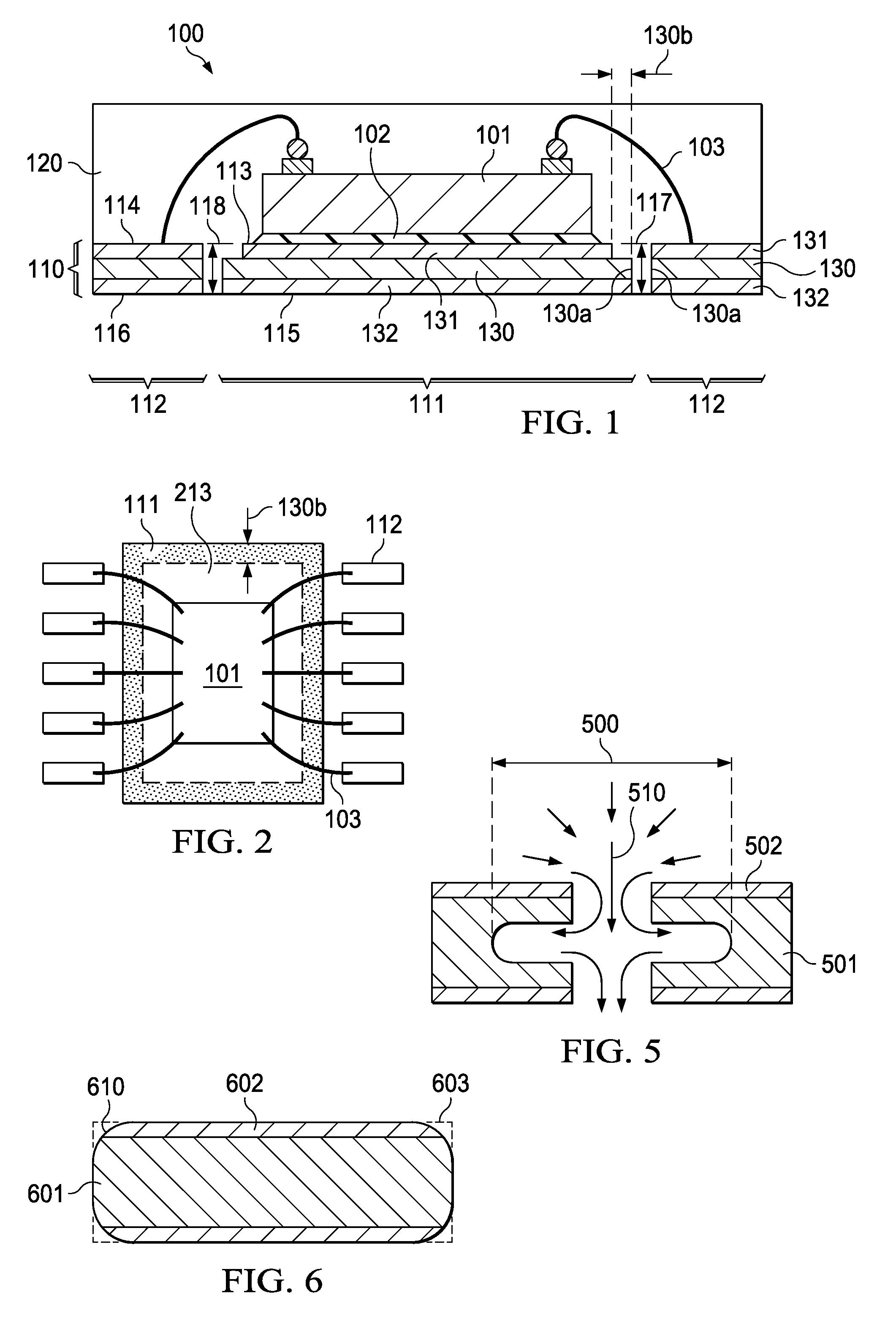
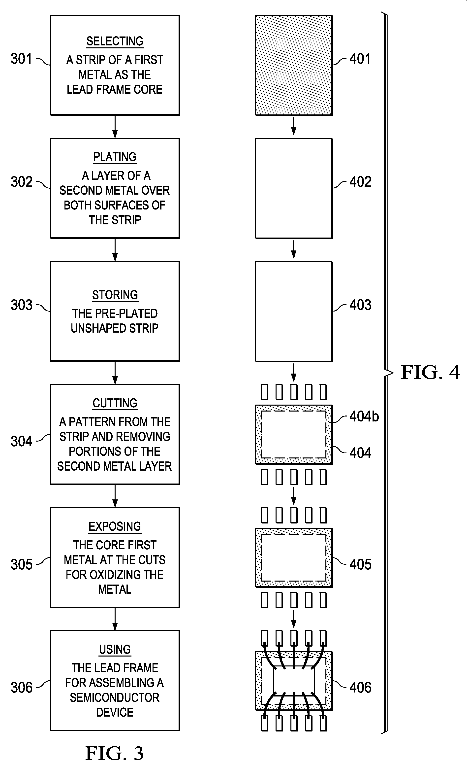
[0021]FIG. 1 depicts an exemplary semiconductor device of the Quad Flat No-Lead (QFN), or Small Outline No-Lead (SON) type, generally designated 100, as an embodiment of the invention. A semiconductor chip 101 is attached by a polymeric material 102 to the pad 111 of a metallic leadframe 110. Besides pad 111, the leadframe 110 has a plurality of leads 112. Pad 111 has a first surface 113 and a second surface 115, which is parallel to first surface 113. Leads 112 have a first surface 114 and a second surface 116, which is parallel to first surface 114. In FIG. 1, first surface 113 of the pad and first surface 114 of the leads lie in one plane, and second surface 115 of the pad and second surface 116 of the leads lie in another parallel plane. In other semiconductor devices, pad 111 and leads 112 may be offset relative to each other so that the pad first surface is in a plane different from but parallel to the plane of the lead first surfaces.

[0022]Pad 111 further has sidewalls 117 or...


PUM

PropertyMeasurementUnit
thickaaaaaaaaaa
delivery timeaaaaaaaaaa
thicknessaaaaaaaaaa

Abstract

A method for fabricating a leadframe for a QFN / SON semiconductor device by selecting (301) a strip of a first metal as the leadframe core, then plating (302) a layer of a second metal over both surfaces of the strip, then cutting (304) a pattern from the pre-plated strip and further removing (304) portions of the second metal layer over a surface to expose the underlying core first metal. The exposed core first metal oxidized (305) before using (306) the leadframe for assembling the semiconductor device. The steps of cutting and removing are performed programmable machining techniques such as computer numerical controlled tools (CNC), electrical discharge machining (EDM), laser cutting, and water jet cutting.

Description

FIELD OF THE INVENTION[0001]The present invention is related in general to the field of semiconductor devices and processes, and more specifically to the structure and fabrication method of semiconductor leadframes for low volume, yet high diversity Quad Flat No-Lead (QFN) and Small Outline No-Lead (SON) devices.DESCRIPTION OF RELATED ART[0002]The metallic leadframes used in semiconductor devices such as dual-in-line devices, surface mount devices, and Quad Flat No-Lead (QFN) and Small Outline No-Lead SON) devices, provide a pad for stable support of the semiconductor chip, and a plurality of leads to bring electrical conductors in close proximity of the chip. After attaching the chip onto the pad, the remaining gap between the chip and a lead is usually bridged by a thin wire attached in a bonding process; the wires are typically made of gold or copper. In order to protect the sensitive chip and wires from environmental disturbances such as moisture, scratches and light, the assemb...

Claims


Application Information

Patent Timeline
Patent Type & Authority Applications(United States)
IPC IPC(8): H01L23/48H01L23/495H01L21/50
CPCH01L21/4842H01L2924/01028H01L23/49582H01L24/45H01L2224/48091H01L2224/48465H01L2224/49171H01L2224/85439H01L2924/01013H01L2924/01029H01L2924/01046H01L2924/01078H01L2924/01079H01L23/3107H01L2224/73265H01L2224/45144H01L2224/32245H01L24/48H01L24/49H01L2224/48247H01L2924/01019H01L2924/00015H01L2924/15747H01L2924/00014H01L2924/00012H01L2924/00H01L2224/45147H01L24/73H01L2224/48639H01L2924/181
Inventor KODURI, SREENIVASAN K.
Owner TEXAS INSTR INC
Why Eureka
Try Eureka