Camera module, and photosensitive component thereof and manufacturing method therefor

a technology of camera modules and photosensitive components, applied in the field of camera modules, can solve the problems of increasing the defective rate restricting the development increasing the thickness of the camera module, so as to reinforce the electromagnetic immunity of the photosensitive unit and the structural strength of the main circuit board

Inactive Publication Date: 2019-05-16
NINGBO SUNNY OPOTECH CO LTD
View PDF0 Cites 16 Cited by
  • Summary
  • Abstract
  • Description
  • Claims
  • Application Information

AI Technical Summary

Benefits of technology

[0107]According to an embodiment of the present invention, the manufacturing method further comprises the following step: attaching a reinforced layer on the main circuit board, so as to reinforce the structural strength of the main circuit board.
[0108]According to an embodiment of the present invention, the manufacturing method for the photosensitive unit further comprises the following step: covering a shielding layer on the encapsulation portion and the main circuit board, so as to reinforce the electromagnetic immunity of the photosensitive unit.

Problems solved by technology

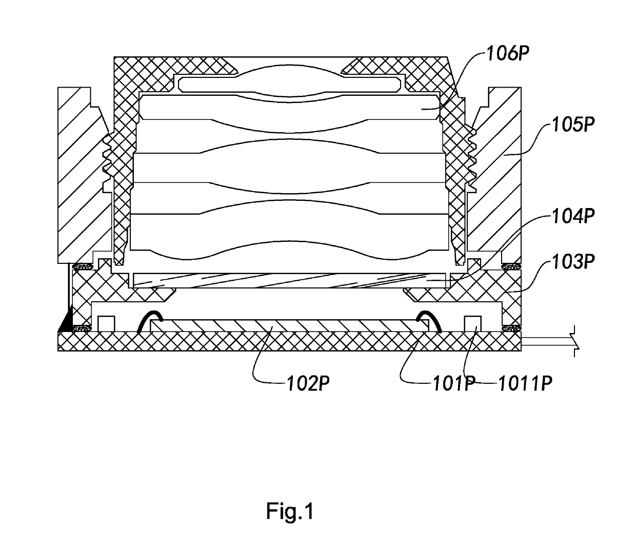
According to the conventional COB technology, there are disadvantages in the assembling and coordination relationships among the circuit board 101P, the circuit components 1011P, and the frame 103P, which also restrict the development for the camera module to become lighter and thinner.
Besides, because the circuit components 1011P and the sensor 102P are connected and provided in a common space, those dusts and pollutants can easily and adversely affect the sensor 102P that can result in undesirable occurrences such as dark spots of the assembled camera module, which increases the defective rate of the camera module.
Therefore, to mount the frame 103P on the circuit board 101P, a safe distance is required to be reserved between the frame 103P and the circuit components 1011P in both horizontal direction and upward direction, that results in increasing the thickness of the camera module and the difficulty to the thickness reduction of the camera model.
Nevertheless, this adjustment space requirement will not only further increase the thickness of the camera module, rendering it substantially being more difficult to reduce the thickness of the camera module, but also cause tilt discrepancy of the assembling more easily during such multiple adhering process.
Due to the limitation in material selection and manufacturing technique, the evenness and flatness of the surface of the frame 103P itself are relatively poor.
As a result, the stability, evenness, and flatness of the bonding between the frame 103P and the circuit board 101P are relatively poor.
Besides, the evenness and flatness of the installing platform for other components, such as the motor unit 105P and / or camera lens 106P, provided by the frame 3P are also poor.
As a result, the size of the electronic device becomes larger and larger, the assemble difficulty thereof increases accordingly, and the overall size of the camera module becomes bigger and bigger.
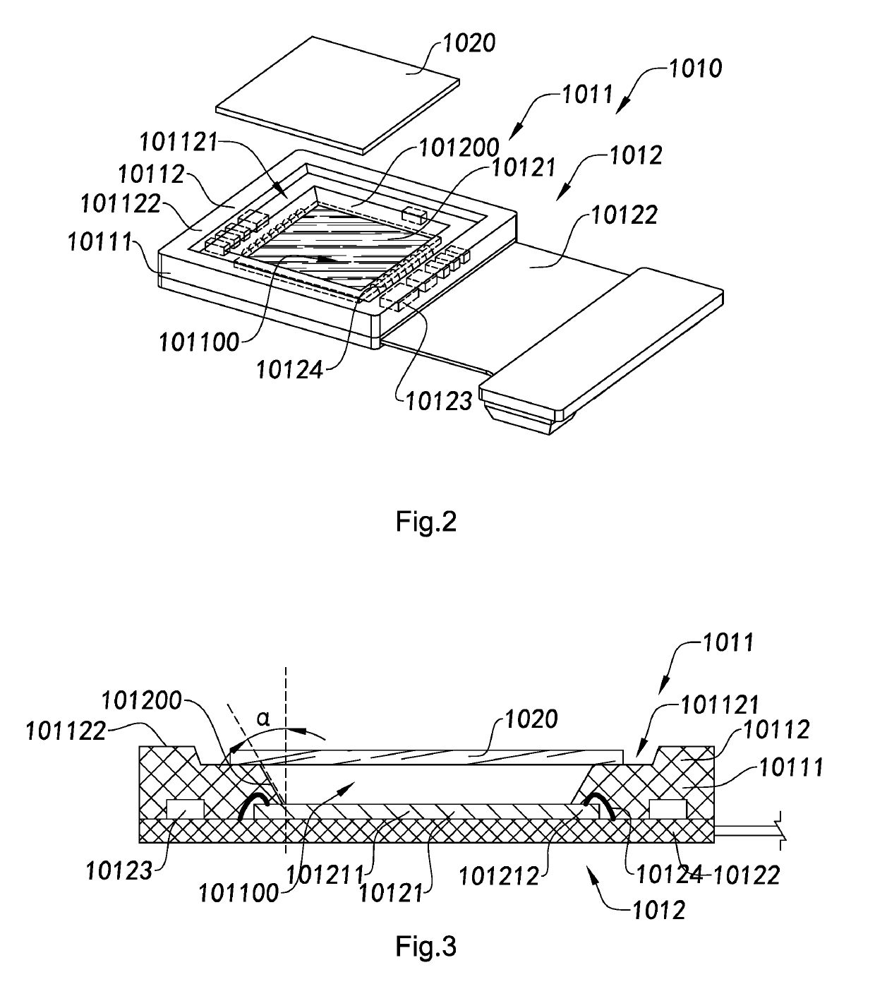
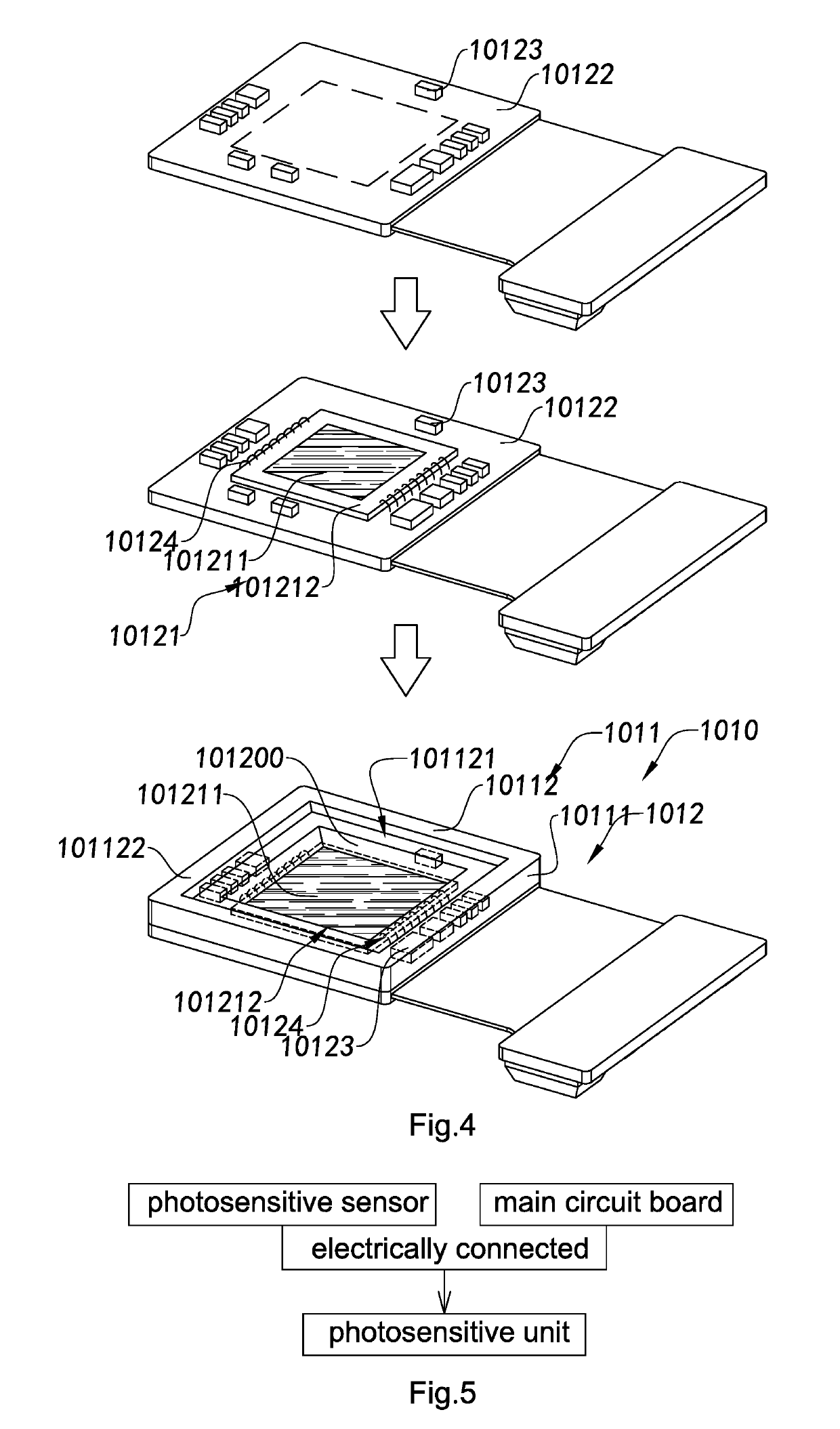
1. The plastic frame is formed alone and then bonded on the circuit board through adhesive. Nonetheless, if the plastic frame is not flat and smooth itself or is assembled with tilt, it will render module tilt. The resistance-capacitance components and the photosensitive sensor all exist in the same space. Because dusts on the resistance-capacitance components cannot be cleaned up easily, it will eventually affect the module and cause dark spots and defectives. The structural strength is weak in circuit board. It is difficult to reduce the product size, especially the lateral dimension thereof. It wastes the dimensions between two camera modules and affects the overall dimensions.
Hence, the ways to reduce the size of the camera module and to enhance the image quality of the camera module have become critical technical issues the camera module industry focuses on recently.
Although this method is positive in enhancing the structural strength of the camera module and reducing the size of the camera module, such camera module manufacturing process still has several issues.
Because the microlenses are usually in a micrometer scale, they can be damaged or scratched very easily.
Especially, the risk is even higher under high temperature and high pressure.
Any microlens of a regular photosensitive sensor being damaged or scratched will inevitably affect the image quality of the camera module.
Because the temperature of the molding material is high, if the molding material flows to the photosensitive area of the photosensitive sensor, it will inevitably damage the microlenses on the photosensitive area of the photosensitive sensor.
Moreover, the burr of the frame may also partially obstruct or shade the photosensitive area of the photosensitive sensor and render defective of the product.
In other words, it is difficult to control both the amount and shape of the glue colloid 503P in this process.
In addition, the bonding stability of the chip 501P and the circuit board 502P in this way is relatively poor.
In other words, the chip 501P can easily be separated from the circuit board 502P due to external force, which is not quite reliable.
Consequently, such pressing is likely to make the chip 501P tilt or even crack the fringe of the chip 501P due to uneven stress.
Unfortunately, it still cannot completely solve the problems, such as inconsistency of the photosensitive axis, poor resolution, abnormal image curve, error code of the motor brought by conventional D / A technique for the camera module.

Method used


Image

  • Camera module, and photosensitive component thereof and manufacturing method therefor
  • Camera module, and photosensitive component thereof and manufacturing method therefor
  • Camera module, and photosensitive component thereof and manufacturing method therefor

Examples


Embodiment Construction

[0244]The following is disclosed in order that those skilled in the art can implement the present invention. Preferred embodiments in the following descriptions are to give examples only. Those skilled in the art can think of other obvious modifications. The basic notions of the present invention defined in the following descriptions can apply to other implementations, modifications, improvements, equivalences, and other technical solutions that do not deviate from the scope or spirit of the present invention.

[0245]Those skilled in the art should understand that in the disclosure of the present invention, terms such as “longitudinal,”“lateral,”“upper,”“lower,”“front,”“back,”“left,”“right,”“perpendicular,”“horizontal,”“top,”“bottom,”“inner,”“outer,” etc., which indicate directions or positional relations are based on the directions or positional relations demonstrated in the figures and only to better describe the present invention and simplify the description, rather than to indicat...


PUM


Abstract

A camera module and photosensitive component or unit thereof and manufacturing method therefor are provided. The photosensitive unit includes an encapsulation portion and a photosensitive portion that includes a main circuit board and a photosensitive sensor, wherein the encapsulation portion is integrally encapsulated to form on the main circuit board and the photosensitive sensor.

Description

CROSS REFERENCE OF RELATED APPLICATION[0001]This is a U.S. National state non-provisional application under 35 U.S.C. § 371 of the international application PCT / CN2017 / 076041, international filing date Mar. 9, 2017, the entire content of which is expressly incorporated herein by reference.NOTICE OF COPYRIGHT[0002]A portion of the disclosure of this patent document contains material which is subject to copyright protection. The copyright owner has no objection to any reproduction by anyone of the patent disclosure, as it appears in the United States Patent and Trademark Office patent files or records, but otherwise reserves all copyright rights whatsoever.BACKGROUND OF THE PRESENT INVENTIONField of Invention[0003]The present invention relates to the field of camera module, and more particularly to a camera module, and photosensitive component or unit thereof and manufacturing method therefor.Description of Related Arts[0004]COB (Chip On Board, chip packaging) technique is a very impo...

Claims


Application Information

Patent Timeline
Patent Type & Authority Applications(United States)
IPC IPC(8): H01L27/146H05K1/02H04N5/225H05K1/11
CPCH01L27/14618H05K1/0274H04N5/2254H01L27/14621H05K1/118H01L27/14698H01L23/10H01L2224/83101H01L2224/83192H01L2224/92247H01L2924/16195H04N23/57H04N23/54H04N23/55
Inventor WANG, MINGZHUZHAO, BOJIETANAKA, TAKEHIKOLUAN, ZHONGYUCHEN, ZHENYUHUANG, ZHEN
Owner NINGBO SUNNY OPOTECH CO LTD
Why Eureka
Try Eureka