Power semiconductor module, power conversion device using same, and method for manufacturing power conversion device

Active Publication Date: 2019-05-23
HITACHI ASTEMO LTD
View PDF0 Cites 1 Cited by
  • Summary
  • Abstract
  • Description
  • Claims
  • Application Information

AI Technical Summary

Benefits of technology

[0007]According to the present invention, miniat

Problems solved by technology

The power semiconductor element generates heat by energization, and thus

Method used


Image

  • Power semiconductor module, power conversion device using same, and method for manufacturing power conversion device
  • Power semiconductor module, power conversion device using same, and method for manufacturing power conversion device
  • Power semiconductor module, power conversion device using same, and method for manufacturing power conversion device

Examples


Example

EXAMPLE 1

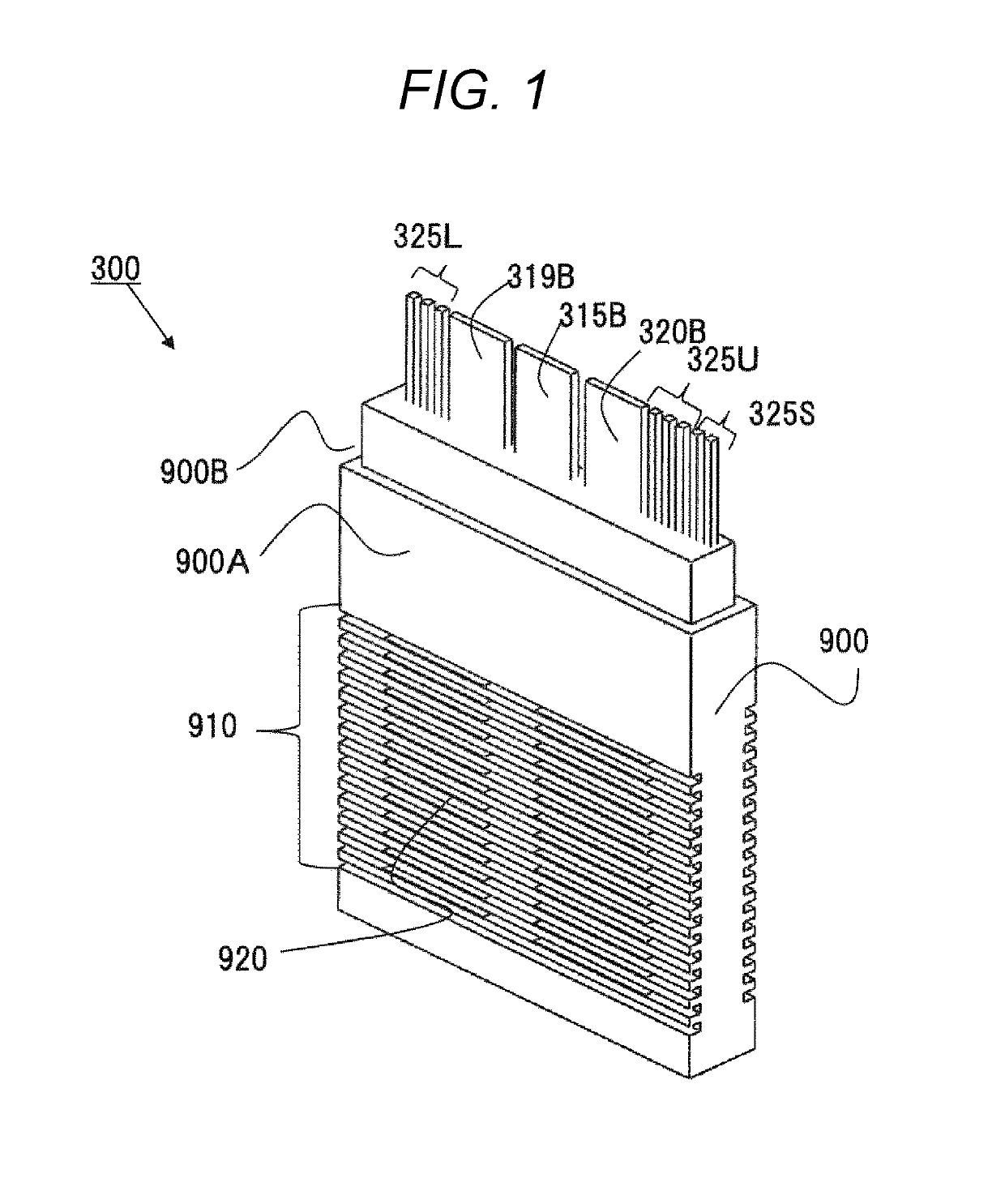
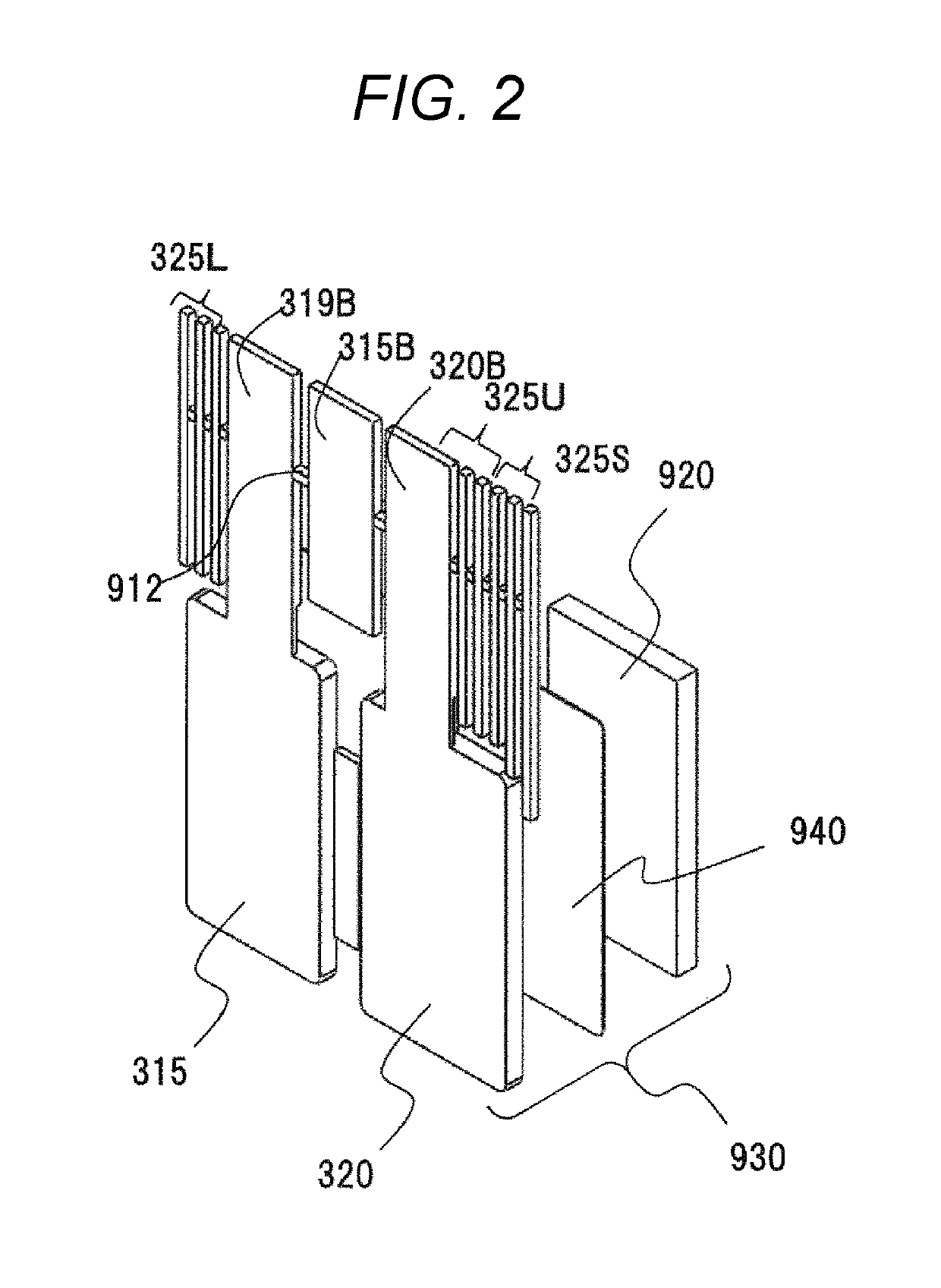
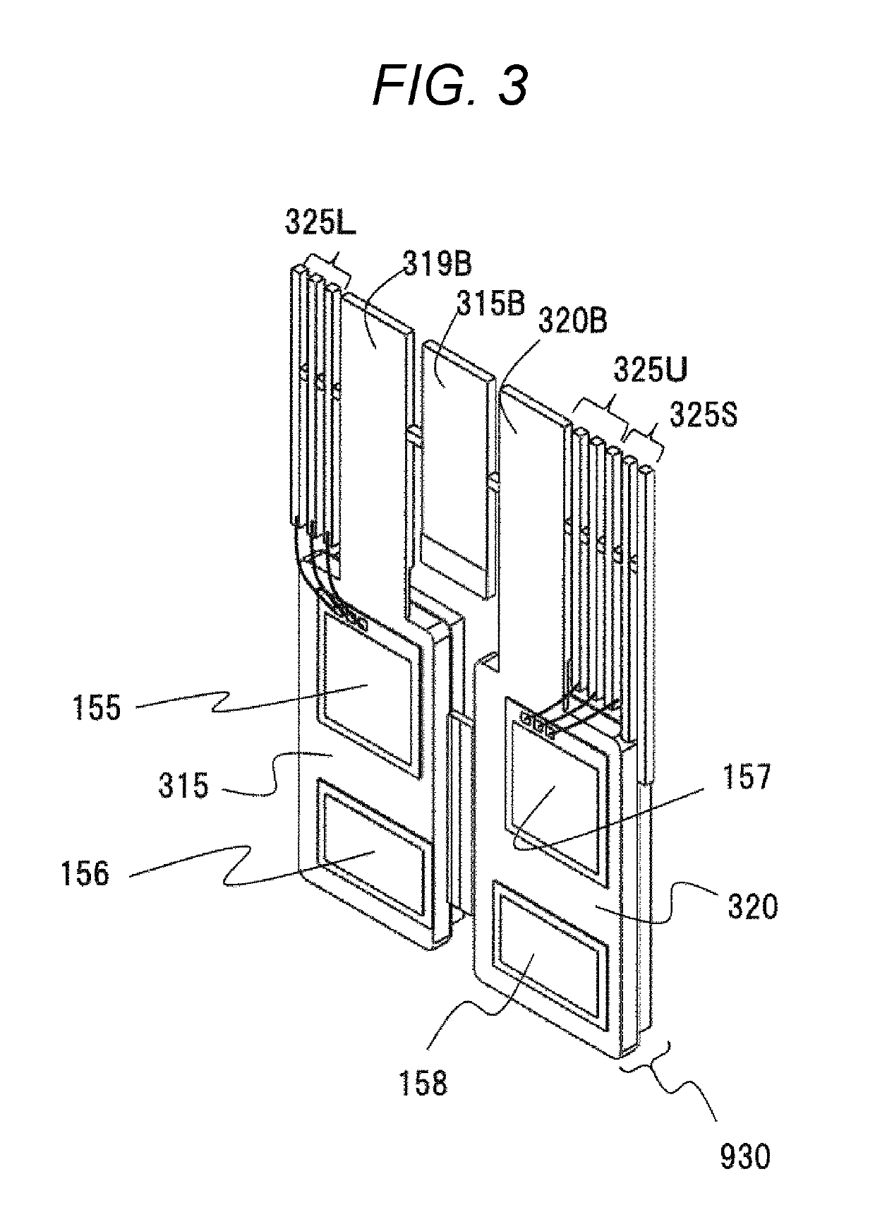
[0032]FIG. 1 is a perspective view of a power semiconductor module 300 of the present embodiment. The power semiconductor module 300 includes: a sealing resin 900 as a case that houses a power semiconductor; terminals 315B and 319B on a DC side; a terminal 320B on an AC side; and signal terminals 325U, 325L, and 325S.

[0033]The sealing resin 900 seals a power semiconductor element mounted on a metal conductor such as a lead frame 315 and a ceramic substrate wiring to be described later. The terminal 315B, the terminal 319B, and the terminal 320B protrude from one surface of the sealing resin 900 and are arranged in a line such that side surfaces of adjacent terminals oppose each other. A step, configured to form a seal structure in a seal portion 900B, is formed on the sealing resin 900 on a side where these terminals protrude.

[0034]When the power semiconductor module 300 is fixed to a flow path forming body 1000, a first fixing material 901 and a second fixing material 902 ...

Example

EXAMPLE 3

[0075]FIG. 16 is a schematic view illustrating a sectional structure of the power conversion device 200 according to a third embodiment. A difference from the first embodiment is that a urethane resin cured product having an elastic modulus of 2 MPa is used as the first fixing material 901 and a resin plate having an elastic modulus of 18 GPa consisting of PPS mechanically fixed to the flow path forming body 1000 is used as the second fixing material 902. As the urethane resin, a two-component waterproof urethane resin was used. A curing condition is two hours at 100° C. Since the second fixing material is mechanically fixed, there is an effect that production speed is high. In addition, a urethane resin is superior in reactivity to an epoxy resin, and thus, there is an effect that it is possible to reduce energy required for the effect. The urethane resin as the first fixing material 901 is injected from above the second fixing material 902. As a result, there is an effect...

Example

EXAMPLE 4

[0077]FIG. 18 is a schematic view illustrating a sectional structure of the power conversion device 200 according to a fourth embodiment. A change point from the first embodiment is that the first fixing material 901 and the second fixing material 902 are graded materials. A urethane resin having an elastic modulus of 2 MPa was applied in advance, and then, an epoxy resin was applied in an uncured state. The urethane resin and the epoxy resin were partially compatible in the vicinity of an interface to become a graded material. Since the first fixing material 901 and the second fixing material 902 are partially compatible, the first fixing material 901 and the second fixing material 902 are in close contact with each other so that an effect that the second fixing material 902 suppresses displacement of the first fixing material 901 is high.


PUM


Abstract

Provided is a compact power conversion device which is excellent in liquid tightness and has high reliability of a terminal connection portion. A power conversion device according to the present invention includes: a case that houses a power semiconductor; a flow path forming body that forms a flow path with an outer surface of the case; a first fixing material in contact with a refrigerant flowing in the flow path; and a second fixing material that is in contact with the first fixing material and the flow path forming body and covers a direction of displacement of the case of the first fixing material caused by water pressure.

Description

TECHNICAL FIELD[0001]The present invention relates to a power semiconductor module, a power conversion device using the same, and a method for manufacturing the power conversion device, and more particularly to a power conversion device including a power semiconductor module having a power semiconductor element.BACKGROUND ART[0002]Power conversion devices using switching of power semiconductor elements have high conversion efficiency, and thus, have been widely used for consumer use, automotive use, railway use, substation equipment, and the like. The power semiconductor element generates heat by energization, and thus, requires high power dissipation and is cooled by using air or a liquid. In particular, a power semiconductor module having a large heat generation uses a cooling system using a liquid, and thus, it is important to provide a seal that secures liquid tightness of a refrigerant flow path on which the power semiconductor module is mounted. PTL 1 is disclosed as a structu...

Claims


Application Information

Patent Timeline
IPC IPC(8): H01L23/473H01L23/00H01L21/52H02M7/00H02M7/537
CPCH01L23/473H01L24/29H01L24/33H01L21/52H02M7/003H02M7/537H01L2224/29191H01L25/07H01L25/18H05K7/20H01L2224/05554H01L2224/33H01L2224/48091H01L2224/48247H01L23/24H01L2924/00H01L2924/00012H01L2924/00014H01L2224/73265H01L2924/0002H01L2924/181
Inventor TSUYUNO, NOBUTAKEKUWANO, MORIOTOKUYAMA, TAKESHI
Owner HITACHI ASTEMO LTD
Why Eureka
Try Eureka