Optical modulator and optical transmission device using the same

a technology of optical modulator and optical transmission device, which is applied in the direction of optics, fibre transmission, instruments, etc., can solve the problems of deterioration of reliability, significant heat generated in the terminal substrate, and temperature drift in the optical modulator

Active Publication Date: 2019-05-30
SUMITOMO OSAKA CEMENT CO LTD
View PDF3 Cites 0 Cited by
  • Summary
  • Abstract
  • Description
  • Claims
  • Application Information

AI Technical Summary

Benefits of technology

[0014]In view of above description, an optical modulator of the disclosure and an optical transmission device using the same are provided. The optical modulator includes an optical waveguide substrate wherean optical waveguide is formed; a control electrode that is provided on the optical waveguide substrate and applies an electric field to the optical waveguide; and a relay substrate that is disposed in the vicinity of the optical waveguide substrate and includes electrical wirings for relaying electrical signals from the outside to the control electrode. The control electrode includes a signal electrode. The optical modulator comprises terminating units that include terminal resistors that terminate the signal electrode. At least a part of the terminating units are provided on the relay substrate.

Problems solved by technology

However, in order to cope with the demand for reducing the size of an optical modulator, it is necessary for the terminal substrate 7 to be disposed in the vicinity of the optical waveguide substrate 1, and heat generated in the terminal substrate is a significant problem.
Heat generated in the terminal substrate causes deterioration in temperature drift in the optical modulator.
In addition, heat generated in the terminal resistors themselves is a cause of deterioration, cracking and separation of the terminal resistors over time, and causes serious problems such as deterioration of the reliability of the optical modulator and an optical transmission device using the same.
However, in the related art, these problems have not been studied yet and countermeasures have not been taken.
Rather, the influence of heat generated becomes lost in change in temperature of an environment in which an optical modulator is placed and instability of the optical modulator and is treated as a problem of deterioration of characteristics such as temperature drift in an optical modulator in the related art.
However, regarding this influence, the influence is particularly large in an optical modulator having a DP-QPSK configuration, in which (a) amplitudes of input electrical signals are large, (b) a plurality of terminal resistors is included, and (c) the terminal resistors are provided on the same substrate, and the problem has become more serious.
Furthermore, the influence becomes more serious due to that the optical modulator has (d) a small size, and (e) a plurality of elements (multi-element configuration).
However, in such a configuration and method, the size of the terminal substrate itself increases and production costs also increase, and the suitable applications are thus limited.

Method used


Image

  • Optical modulator and optical transmission device using the same
  • Optical modulator and optical transmission device using the same
  • Optical modulator and optical transmission device using the same

Examples


third embodiment

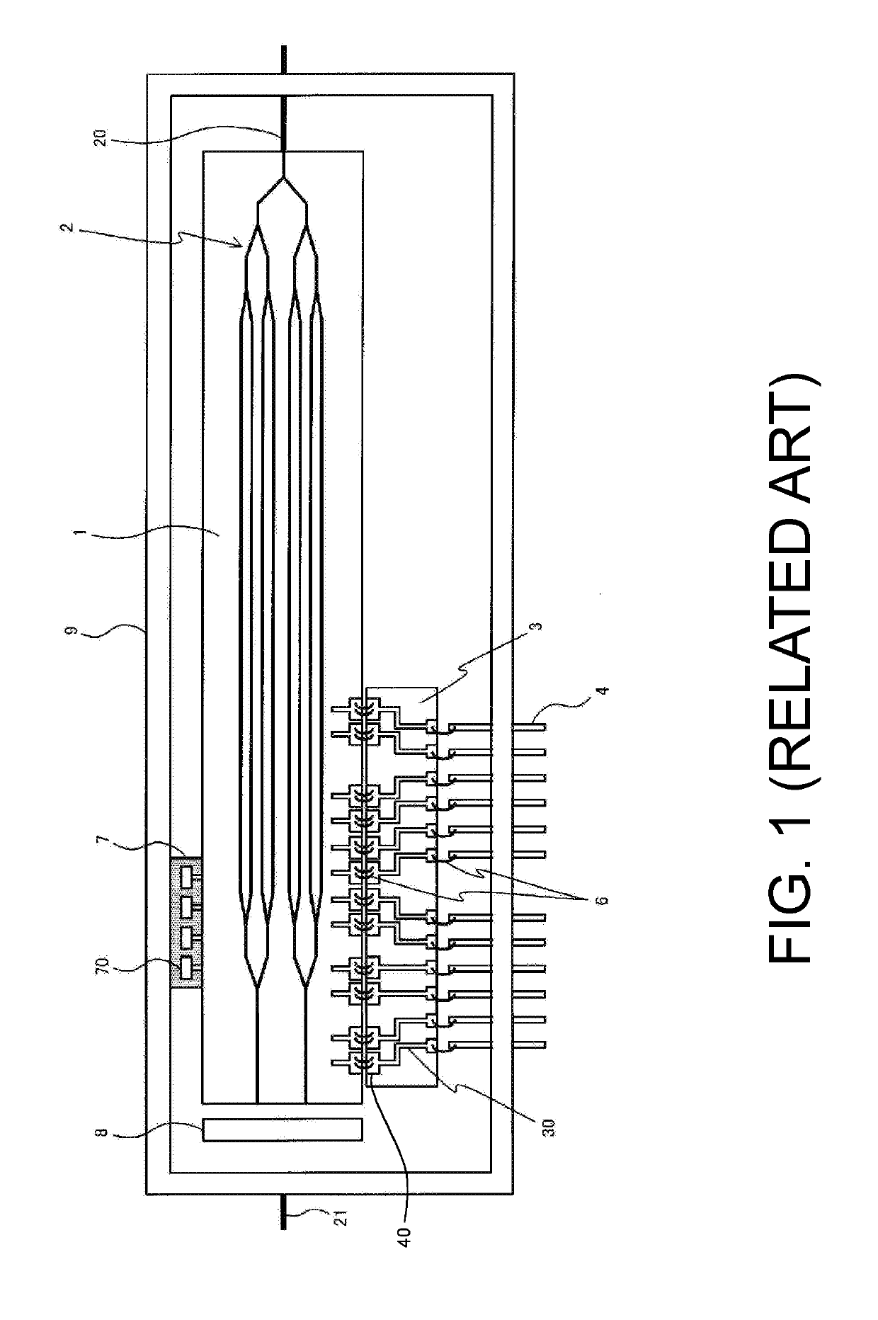
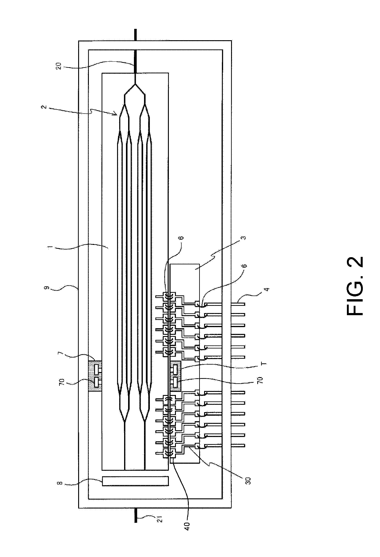
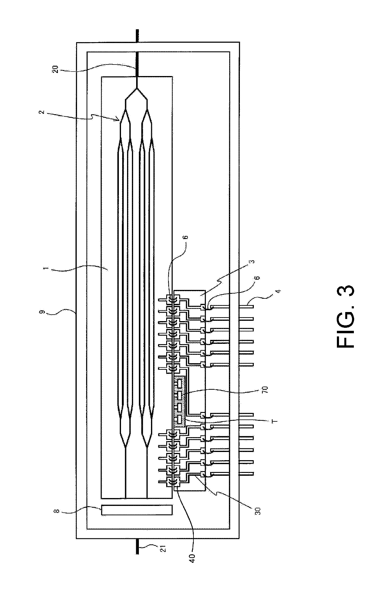
[0037]In the disclosure, as shown in the third embodiment in FIG. 4, when the terminating unit T and the electrical wirings 31 for light reception are disposed on the same relay substrate 3, a configuration may be adopted that the terminating unit T and the electrical wirings 31 for light reception are disposed to be separated by a gap, and the high frequency signals leaking from the terminating unit T do not enter the electrical wirings 31 for light reception.

fourth embodiment

[0038]When the light receiving elements PD are provided, as shown in the fourth embodiment in FIG. 5, a configuration may be used that a relay substrate is formed of two substrates 33 and 34, and the substrate 33 where the terminating unit T is provided and the substrate 34 where the electrical wirings 31 for light reception are separately formed. In this manner, when the substrates 33, 34 are different from each other, it is possible to effectively suppress the high frequency signals from entering the electrical wiring 31.

fifth embodiment

[0039]In addition, as shown in the fifth embodiment in FIG. 6, electrical wirings for light reception may not be formed in the relay substrate 3, and can be replaced with wire bondings 6. Although the number of processes slightly increases due to bonding, it is then possible to greatly increase the degree of freedom in design such as a layout design of the light receiving elements PD and a layout design of various wiring patterns and the like, and it is possible to isolate the relay substrate 3 where signal lines of the light receiving elements PD and the terminal resistors are formed. Here, in FIGS. 5 and 6, the input / pins 41 outputs the detection signals of the light receiving elements PD. Input / output pins 43 supply a DC bias voltage. Input / output pins 44 mainly supply electrical signals for modulation. Here, a part of the input / output pins 44 may be used for DC bias.

[0040]In addition, as shown in FIGS. 7 to 9, at least one of an electrical wiring 33 for relaying a DC bias voltag...


PUM

PropertyMeasurementUnit
thicknessaaaaaaaaaa
electric fieldaaaaaaaaaa
DC bias voltageaaaaaaaaaa

Abstract

A small and inexpensive optical modulator having suppressed temperature drift and high reliability and an optical transmission device using the same are provided. The optical modulator includes an optical waveguide substrate where an optical waveguide is formed; a control electrode that is provided on the optical waveguide substrate and applies an electric field to the optical waveguide; and a relay substrate that is disposed in the vicinity of the optical waveguide substrate and includes electrical wirings that relay electrical signals from the outside to the control electrode. The control electrode includes a signal electrode. The optical modulator comprises terminating units that include terminal resistors that terminate the signal electrode. At least a part of the terminating units are provided on the relay substrate.

Description

CROSS-REFERENCE TO RELATED APPLICATION[0001]The present application is related to and claims priority from Japanese patent application no. 2017-230088, filed on Nov. 30, 2017. The entire contents of the aforementioned application are hereby incorporated by reference herein.BACKGROUNDTechnical Field[0002]The disclosure relates to an optical modulator and an optical transmission device using the same, and particularly, to an optical modulator including a terminating unit in which terminal resistors are disposed at a termination of a signal electrode and an optical transmission device using the same.Description of Related Art[0003]In recent years, in high speed / large capacity optical fiber communication systems, optical modulators using a substrate in which an optical waveguide is formed and optical transmission devices into which such optical modulator is incorporated have been widely used. With regard to these, an optical modulator in which LiNbO3 (referred to as “LN”) having an elec...

Claims


Application Information

Patent Timeline
Patent Type & Authority Applications(United States)
IPC IPC(8): G02F1/225G02F1/035H04B10/25H04B10/516
CPCG02F1/225G02F1/035H04B10/2504H04B10/5161G02F2001/212H04B10/532H04B10/5561G02F2203/21G02F1/0305G02F1/0316G02F1/212H04B10/25891
Inventor MIYAZAKI, NORIKAZUSUGAMATA, TORU
Owner SUMITOMO OSAKA CEMENT CO LTD
Why Eureka
Try Eureka