Radiation imaging apparatus

a technology of radiation imaging and apparatus, applied in the direction of radiation controlled devices, optical radiation measurement, instruments, etc., can solve the problems of increasing the capacitance of output signal lines, difficult high-speed operations, and difficulty in amorphous silicon, so as to enhance the suppression of thermal influence of control units

Inactive Publication Date: 2012-05-03
CANON KK
View PDF4 Cites 4 Cited by
  • Summary
  • Abstract
  • Description
  • Claims
  • Application Information

AI Technical Summary

Benefits of technology

[0017]At least one embodiment of the present invention is directed to enhancing suppression of thermal influence of a control unit on a radiation flat panel detector, in a radiation imaging apparatus.

Problems solved by technology

However, since semiconductor characteristics are not adequate, it is difficult to perform high-speed operations.
Further, amorphous silicon has more difficulty in microfabrication of semiconductor substrate on the glass substrate, in comparison to single-crystal silicon semiconductor substrate, and as a result, capacitance of output signal lines becomes larger, and kTC noise (thermal noise on capacitors) becomes more likely to be generated.
However, it is unfit to trend toward a larger screen size.
In this case, driving voltages differ between different locations at drive end and near the center, and thus a complete transfer becomes difficult.
C and V tend to become large in large detector areas, thus power consumption becomes up to ten times greater in a CCD image sensor as compared to a CMOS image sensor.
However, the flat panel type of radiation detector, which has used the CMOS image sensor, has amplifiers on a per-pixel basis, and thus thermal noise due to heat generation of the amplifiers has become a problem.
Since images generated by the image sensor are negatively influenced by heat, image quality of the acquired X-ray images may be degraded due to the thermal noise.
Despite of the state of the art described above, even if the heat of the radiation flat panel detector has been dissipated to the external housing by using the technology discussed in Japanese Patent Application Open-Laid No. 2009-085630, when the heat generated from the control unit including electronic components is conveyed to the radiation flat panel detector, it may result in adverse effects on the captured radiation images to be generated.
However, the heat generated from a power source apparatus and other electronics that control an imaging apparatus tend to add up and negatively affect imaging performance therein.
Thus, the countermeasures discussed in Japanese Patent Application Open-Laid No. 2003-194951 and in the above-discussed references have not achieved an optimal solution to address the problems of heat affecting radiation flat panel detectors.
In particular, local temperature rise may occur in the electronic components, and there is a possibility that local noises be generated in the radiation imaging images previously created.

Method used


Image

  • Radiation imaging apparatus
  • Radiation imaging apparatus
  • Radiation imaging apparatus

Examples


Embodiment Construction

[0028]Various exemplary embodiments, features, and aspects of the invention will be described in detail below with reference to the drawings.

[0029]Descriptions of respective exemplary embodiments as below are given assuming a radiation imaging apparatus using the CMOS image sensor in which the need for minimizing thermal influence is high.

[0030]However, the present invention is not limited to the radiation imaging apparatus using the CMOS image sensor, but can be also applied to a radiation imaging apparatuses using other image sensors such as amorphous silicon type, or CCD type.

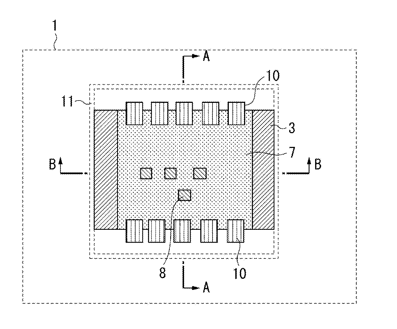
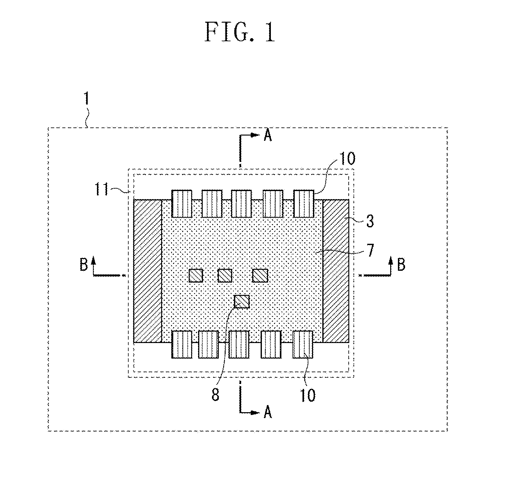
[0031]A first exemplary embodiment will be described. FIG. 1 is a plan view illustrating a radiation imaging apparatus 1 having a surface opposite to X-ray incident side of the radiation imaging apparatus in the present exemplary embodiment. In other words, as illustrated in FIG. 1, X-ray radiation is incident upon the radiation imaging apparatus 1 from the rear side to front side. In FIG. 1, an external hou...


PUM


Abstract

A radiation imaging apparatus includes a radiation flat panel detector configured to detect radiation incident thereupon and to generate a radiation image, a control unit configured to control a drive of the radiation flat panel detector, a heat insulation member arranged between the radiation flat panel detector and the control unit, an external housing configured to accommodate therein the flat panel detector and the control unit, a first heat transfer member configured to transfer heat from the radiation flat panel detector to a first surface of the external housing, and a second heat transfer member configured to transfer heat from the control unit to a second surface of the external housing different from the first surface.

Description

BACKGROUND OF THE INVENTION[0001]1. Field of the Invention[0002]The present invention relates to a radiation imaging apparatus that detects radiation which has passed through an object, and generates a radiation image.[0003]2. Description of the Related Art[0004]In recent years, a flat panel type of radiation imaging apparatus of an same size optical system using photoelectric conversion element has been in widespread use, for the purposes of enhancement of resolutions, reduction in size of housings, and suppression of distortions of images, in the field of a digital radiation imaging apparatus (X-ray imaging apparatus). The imaging apparatuses using the photoelectric conversion elements include amorphous silicon type, charge-coupled device (CCD) type, complementary metal oxide semiconductor (CMOS) type, and the like.[0005](1) Amorphous Silicon TypeAn advantage of the amorphous silicon type of imaging apparatuses includes the ability to easily create an image sensor of a large-scree...

Claims


Application Information

Patent Timeline
Patent Type & Authority Applications(United States)
IPC IPC(8): G01T1/16
CPCH01L27/146G01T1/244
Inventor GONDA, TAKAAKI
Owner CANON KK
Why Eureka
Try Eureka