Transistor finger spacing and dimension variation in electronic devices

a technology of electronic devices and transistors, applied in the field of electronic devices, can solve the problems of uneven voltage division of transistor stacks, non-uniform drain-to-source spacing of transistor stacks, and fets and/or other transistor devices, and achieve the effect of adding capacitan

Active Publication Date: 2019-06-06
SKYWORKS SOLUTIONS INC
View PDF3 Cites 99 Cited by
  • Summary
  • Abstract
  • Description
  • Claims
  • Application Information

AI Technical Summary

Benefits of technology

[0014]In some implementations, the present disclosure relates to a radio-frequency (RF) module comprising a packaging substrate configured to receive a plurality of devices, and a transistor stack mounted on the packaging substrate, the transistor stack including a first field-effect transistor (FET) disposed on the substrate, the first FET having a first plurality of gate fingers separated by a first gate-to-gate distance, and a second FET disposed on the semiconductor substrate in a series connection with the first FET, the second FET having a second plurality of gate fingers separated by a second gate-to-gate distance, the second gate-to-gate distance being greater than the first gate-to-gate distance.
[0015]In certain embodiments, the first and second FETs are silicon-on-insulator (SOI) transistors. The first plurality of gate fingers may be more than the second plurality of gate fingers. The first plurality of gate fingers may have a first gate width that is shorter than a gate width of the second plurality of gate fingers. The first FET may have a total periphery that is greater than a total periphery of the second FET. In certain embodiments, the first FET has a total periphery that is greater than a total periphery of the second FET. The first FET may have a first plurality of drain fingers having second level metal traces electrically coupled thereto to provide added capacitance. The first FET may occupy a smaller physical area than the second FET. In certain embodiments, the RF module further comprises a third FET having a third plurality of gate fingers separated by a third gate-to-gate distance that is greater than the second gate-to-gate distance. The second plurality of gate fingers may have a gate width that is longer than a gate width of the first plurality of gate fingers and shorter than a gate width of the third plurality of gate fingers.

Problems solved by technology

Furthermore, transistor stacks configured with non-uniform drain-to-source spacing may be applicable to switching, amplifying, mixing, or other applications or solutions applications.
FETs and / or other transistor devices may suffer from certain parasitic capacitances due to the underlying substrate (Club) under various conditions.
Therefore, due to the uneven effect of capacitance on the various transistors, uneven voltage division may occur across the stack of transistors.
In FIG. 18, one can readily see that there can be significant imbalance of voltage drop values along the stack.
As described herein, such an uneven voltage distribution along the stack can result in degradation of switch performance with respect to, for example, harmonic peaking, compression point and / or intermodulation distortion (IMD).
Also, at higher power levels, the first FET can go into breakdown before other FETs, thereby limiting the overall performance of the switch.
It is further noted that such an uneven voltage distribution can impact the breakdown voltage performance of the stack.
However, such uniform drain-to-source spacing can lead to the uneven voltage distribution issues described above.
However, in certain embodiments, wherein drain-to-source spacing is not placed at relatively minimal values, which may provide relatively minimal total metal-to-metal capacitance, uneven voltage distribution may result, as described above.
However, it should be understood that such dimensions are not necessarily drawn to scale and may have any desirable or suitable values and still fall within the scope of the present disclosure.
Such a configuration may provide increased total transistor periphery, which may result in reduced ON-resistance and / or reduced loss, while substantially maintaining transistor size.

Method used


Image

  • Transistor finger spacing and dimension variation in electronic devices
  • Transistor finger spacing and dimension variation in electronic devices
  • Transistor finger spacing and dimension variation in electronic devices

Examples


Embodiment Construction

[0062]The headings provided herein are for convenience only and do not necessarily affect the scope or meaning of the claimed invention.

INTRODUCTION

[0063]Disclosed herein are various examples of a field-effect transistor (FET) device having one or more regions relative to an active FET portion configured to provide a desired operating condition for the active FET. In such various examples, terms such as FET device, active FET portion, and FET are sometimes used interchangeably, with each other, or some combination thereof. Accordingly, such interchangeable usage of terms should be understood in appropriate contexts.

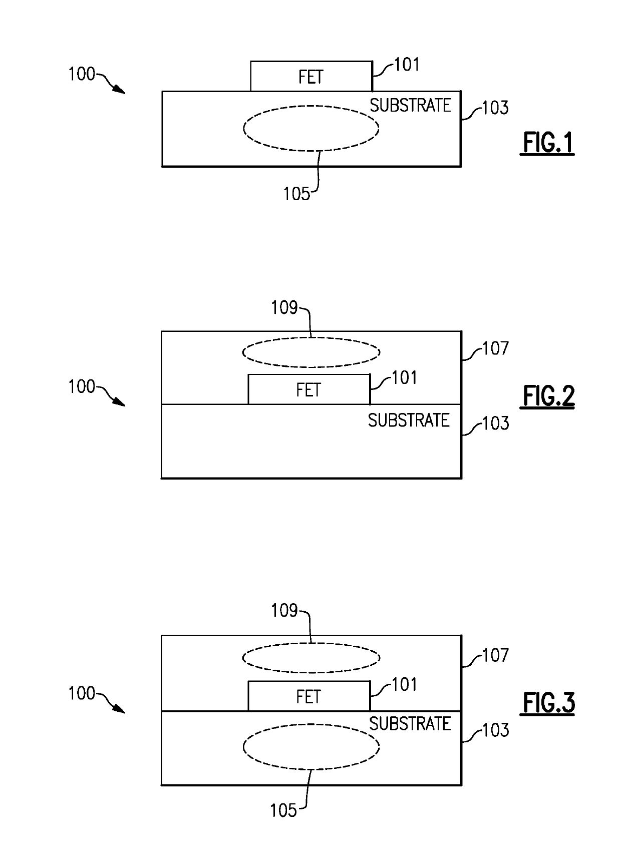
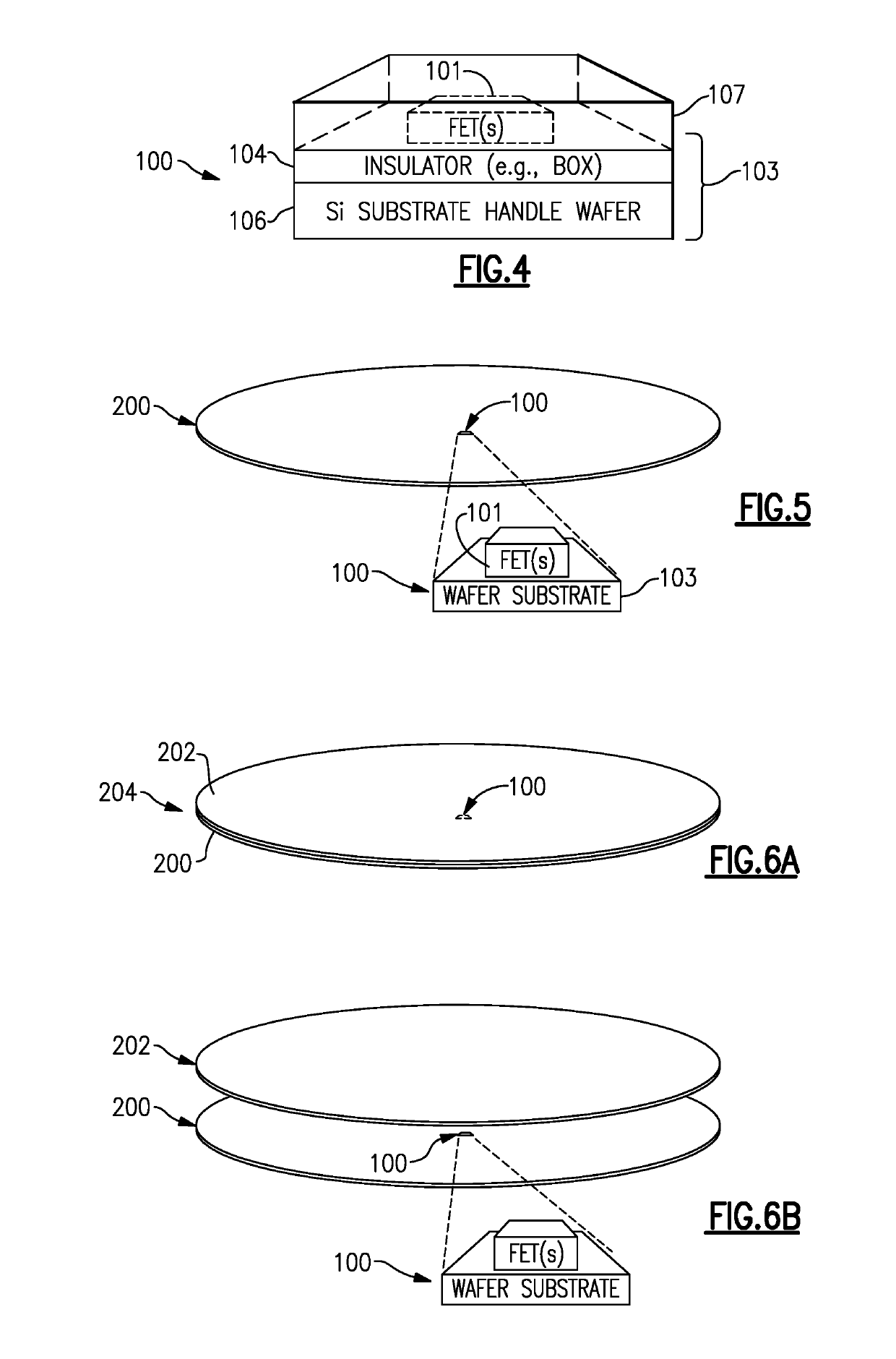
[0064]FIG. 1 shows an example of a FET device 100 having an active FET 101 implemented on a substrate 103. As described herein, such a substrate can include one or more layers configured to facilitate, for example, operating functionality of the active FET, processing functionality for fabrication and support of the active FET, etc. For example, if the FET device 100 is i...


PUM


Abstract

A radio-frequency device comprises a first transistor including a first set of fingers having a first finger-to-finger spacing in a width dimension of the first transistor, and a second transistor in a series connection with the first transistor, the second transistor including a second set of fingers having a second finger-to-finger spacing in the width dimension that is greater than the first finger-to-finger spacing.

Description

CROSS-REFERENCE TO RELATED APPLICATION(S)[0001]This application is a continuation of U.S. patent application Ser. No. 15 / 714,221, filed Sep. 25, 2017, and entitled VOLTAGE DISTRIBUTION IN TRANSISTOR STACKS USING NON-UNIFORM TRANSISTOR DIMENSIONS, which is a continuation of U.S. patent application Ser. No. 15 / 240,771, filed Aug. 18, 2016, and entitled NON-UNIFORM SPACING IN TRANSISTOR STACKS, which claims priority to U.S. Provisional Application No. 62 / 208,540, filed Aug. 21, 2015, and entitled NON-UNIFORM SPACING IN TRANSISTOR STACKS, the disclosures of which are hereby incorporated by reference in its entirety.BACKGROUNDField[0002]The present disclosure generally relates to the field of electronics, and more particularly, to radio-frequency (RF) modules and devices.Description of Related Art[0003]In electronics applications, passive and active devices can be utilized for various purposes, such as for routing and / or processing of radio-frequency (RF) signals in wireless devices.SUMM...

Claims


Application Information

Patent Timeline
Patent Type & Authority Applications(United States)
IPC IPC(8): H01L27/12H01L27/02H01L27/088H01L29/417
CPCH01L27/1203H01L27/0207H01L27/088H01L29/41725H01L29/41733
Inventor WHITEFIELD, DAVID SCOTT
Owner SKYWORKS SOLUTIONS INC
Why Eureka
Try Eureka