Optical sensor module and method for manufacturing an optical sensor module for time-of-flight measurement

a technology of optical sensor module and optical sensor module, which is applied in the direction of instruments, measurement devices, and using reradiation, can solve problems such as time-of-flight value, and achieve the effects of reducing package cost, improving accuracy of time-of-flight measurement, and reducing crosstalk

Active Publication Date: 2019-06-20
AMS AG
View PDF14 Cites 5 Cited by
  • Summary
  • Abstract
  • Description
  • Claims
  • Application Information

AI Technical Summary

Benefits of technology

[0020]The proposed optical sensor module allows for significantly reducing package costs when compared to state of the art systems. For example, a compact form factor can be realized as the reference path resides inside the module. At the same time crosstalk is reduced which leads to improved accuracy of time-of-flight measurements. In fact, due to the arrangement of the optical emitter in the first chamber, the main detector inside the second chamber and the reference detector outside the first chamber, unwanted optical crosstalk from the optical emitter to the detectors, such as the main detector, and light leakage between the chambers may be reduced. This allows for an improved precision of the determined start and / or stop time and consequently of the TOF.
[0021]The apertures can be defined by openings in the cover section. Sizes and locations of these apertures may be controlled precisely, for example by means of a lithographic structuring process or by means of a molding process on the cover section. For example, lithographic structuring can be used to achieve smaller feature sizes and could be more accurately define the apertures when compared to a molding process. Consequently, the reference and measurement paths can be fine-tuned and intensity, position and / or direction of light beams in the optical sensor module can be controlled in a more accurate way. This may further reduce undesired optical crosstalk between the optical emitter and the main detector and thus improve the precision of the measurement.
[0031]In operation, light is coupled into the carrier and is attenuated along the reference path. Even though the carrier material may be opaque there may be some transmission of the emission of the optical emitter. For example, silicon as a carrier material has non zero transmission in the infrared. Attenuation due to reference path in or through the carrier has the benefit to loosen requirements on additional filters, such as optical density (OD) filters. In some embodiments it may even be possible to dispense any additional filters. Furthermore, by using the carrier, or parts thereof, as reference path renders the overall design of the optical module less complex, and, thus, less costly to manufacture.
[0038]The meander structure with the set of interdigitated fingers attenuates light, or optically limits power of light, traversing along the reference path. Thus, the meander reduces optical crosstalk and supports improved measurement accuracy. Furthermore, the meander provides a design option which decouples the housing, e.g. the light barrier, from the carrier. In other words, there may be no direct connection between the light barrier and the carrier due to the interdigitated fingers. This improves stability of the optical sensor module which may be less prone to damage under mechanical stress. Furthermore, no additional connection needs to be provided between the light barrier and the carrier which renders manufacture of the module less complex and, thus, less costly.
[0041]For example, the frame body and the light barrier may not fabricated separately and connected to each other in a separate process step, such as for example by an adhesive. Consequently, undesired leakage of light between the first and the second chamber at interfaces between the light barrier and the frame body may be avoided.

Problems solved by technology

Subtracting both results leads to a time-of-flight value and tends to cancel out systematic errors of the response time of the driver circuit, the light source and readout circuitry.

Method used


Image

  • Optical sensor module and method for manufacturing an optical sensor module for time-of-flight measurement
  • Optical sensor module and method for manufacturing an optical sensor module for time-of-flight measurement
  • Optical sensor module and method for manufacturing an optical sensor module for time-of-flight measurement

Examples


Embodiment Construction

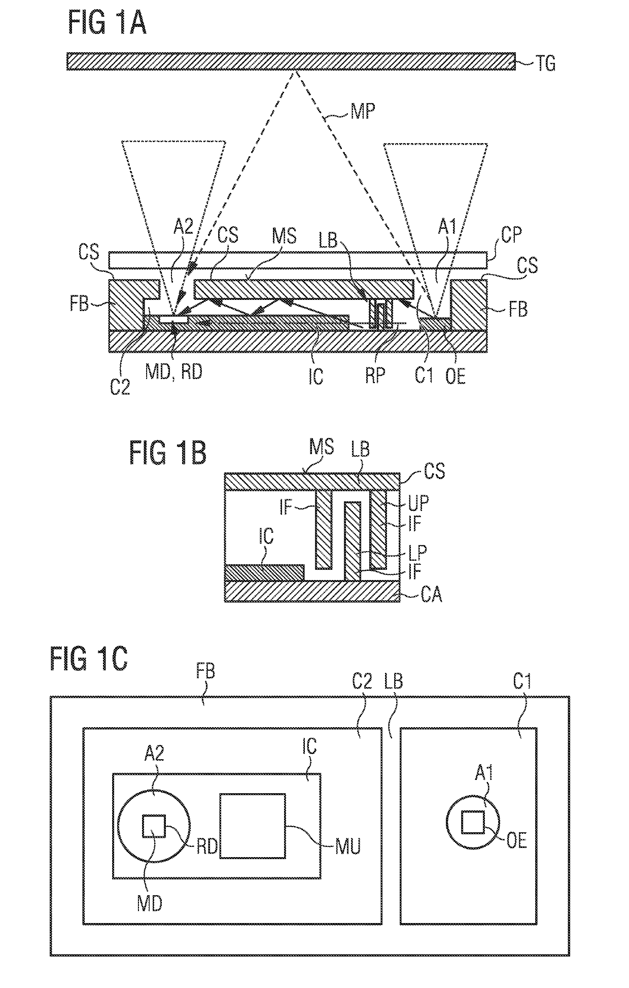
[0062]FIGS. 1A to 1C show an exemplary embodiment of an optical sensor module with a meander structured light barrier.

[0063]FIG. 1A shows a side view of the optical sensor module with the meander structured light barrier LB.

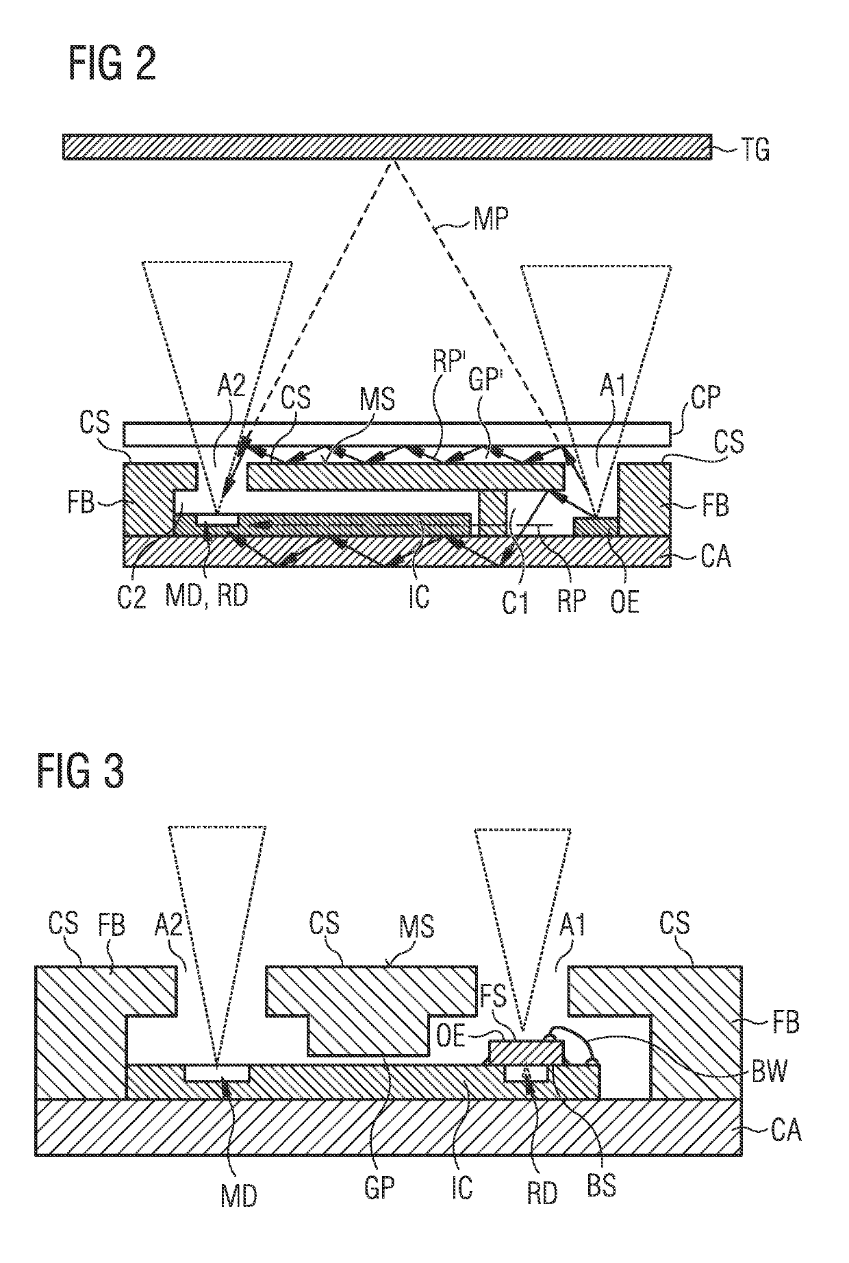
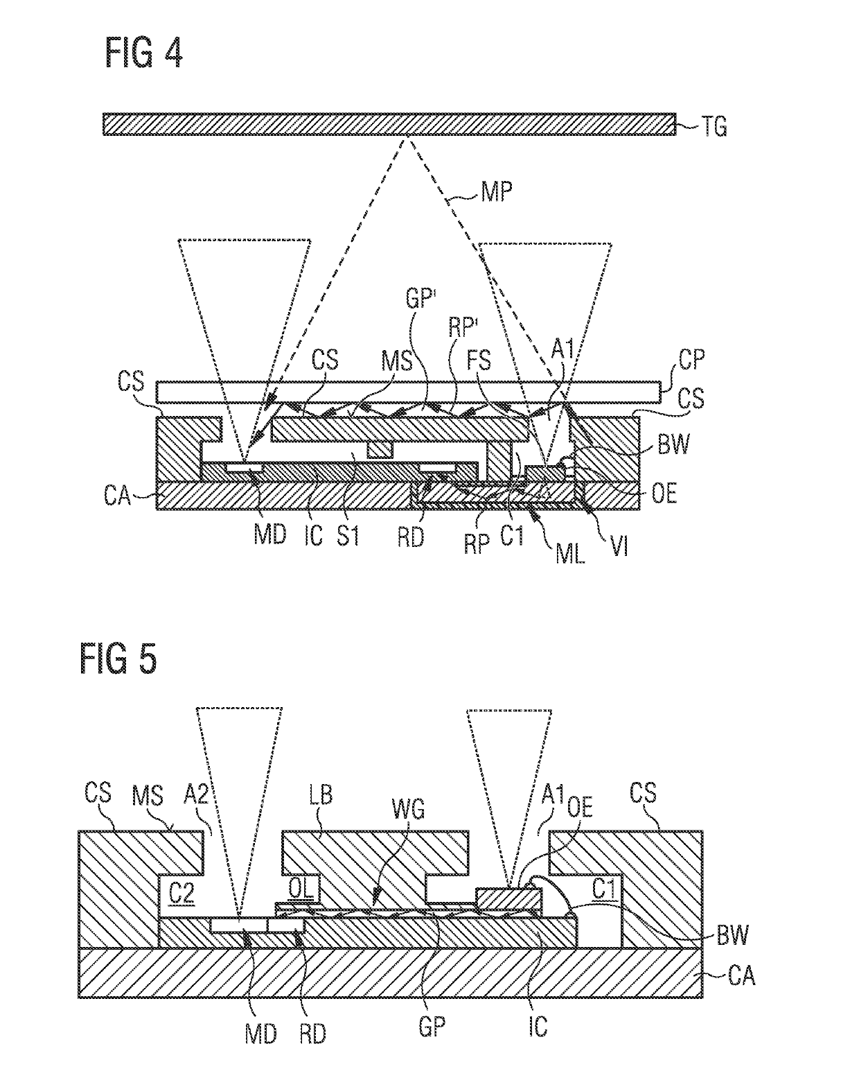
[0064]The module comprises a carrier CA and an opaque housing arranged on the carrier. The housing comprises a light barrier LB which divides the housing into a first and a second chamber C1, C2. The first and second chambers C1, C2 are further confined laterally by a frame body FB arranged in the housing. A cover section CS is located opposite to the carrier CA and thereby covers the chambers C1, C2. The cover section CS has a main surface MS which essentially is parallel to a main surface of the carrier CA. The cover section CS, frame body FB, and light barrier LB are manufactured are all comprised by a continuous piece of material, such as a mold material, for example. The light barrier LB comprises a meander structure of interdigitated fingers which are partl...


PUM


Abstract

An optical sensor module for time-of-flight measurement comprises an optical emitter, a main detector and a reference detector which are arranged in or on a carrier. An opaque housing of the optical sensor module has a first chamber and a second chamber which are separated by a light barrier. The housing has a cover section and is arranged on the carrier such that the optical emitter is located inside the first chamber, the main detector is located inside the second chamber and the reference detector is located outside the first chamber. Furthermore, a main surface of the cover section is positioned opposite the carrier. The optical emitter is arranged and configured to emit light through a first aperture in the cover section, and the main detector is arranged and configured to detect light entering the second chamber through a second aperture in the cover section. A reference path is established between the optical emitter and the reference detector inside the optical sensor module, and confined by the main surface of the cover section and the carrier. Additionally, a method for manufacturing an optical sensor module for time-of-flight measurement is presented.

Description

[0001]This invention relates to an optical sensor module and to a method for manufacturing an optical sensor module, e.g. for time-of-flight measurements.BACKGROUND OF THE INVENTION[0002]Optical sensors for time-of-flight, TOF, measurement find application in various distance measurement systems. Examples include camera autofocus assistance systems, parking assistance systems for vehicles and control or monitoring systems for self-driving vehicles. TOF sensors are often implemented into dedicated sensor modules comprising highly adapted sensor packages. For example, TOF sensor modules typically require an optical reference path and a measurement path in order to accurately detect a time stamp of the light emission and arrival of reflected light, such as a laser beam. Optical sensor modules for TOF often comprise single or arrays of single-photon avalanche diodes, SPAD, as their main optical detector. To achieve high time measurement precision a reference SPAD, or reference SPAD arra...

Claims


Application Information

Patent Timeline
Patent Type & Authority Applications(United States)
IPC IPC(8): G01S7/481G01S17/08G01S7/48
CPCG01S7/4813G01S17/08G01S7/4808G01S7/497
Inventor KAPPEL, ROBERTMANNINGER, MARIOBISHOP, TODD
Owner AMS AG
Why Eureka
Try Eureka