This helps you quickly interpret patents by identifying the three key elements:
Problems solved by technology
Method used
Benefits of technology
Benefits of technology
The present invention aims to provide an electroluminescent display device that can overcome the problem of electrical short between adjacent pads.
Problems solved by technology
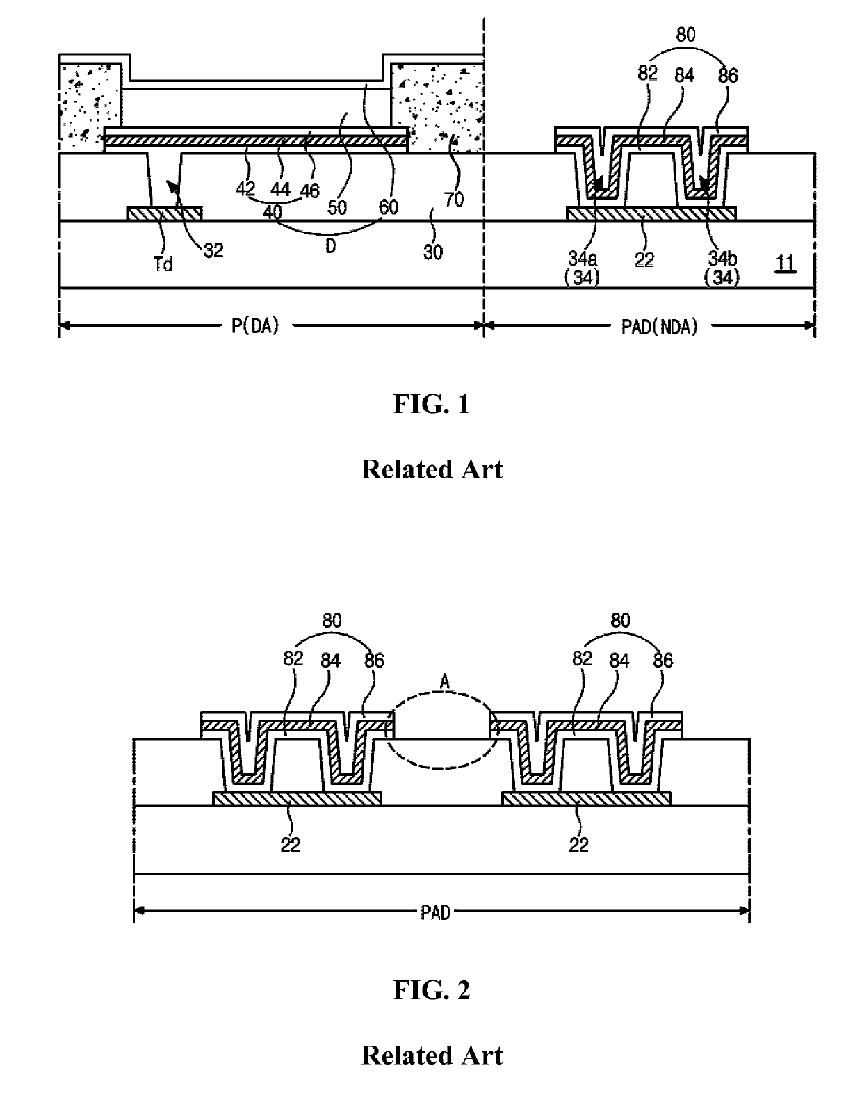
By the way, in the electroluminescent display device 10, an electrical short occurs between adjacent pads 22, and thus there is a problem in driving properties of the electroluminescent display device 10.
Method used
Image
Click on the blue label to locate the original text in one second.
Reading with bidirectional positioning of images and text.
Examples
first embodiment
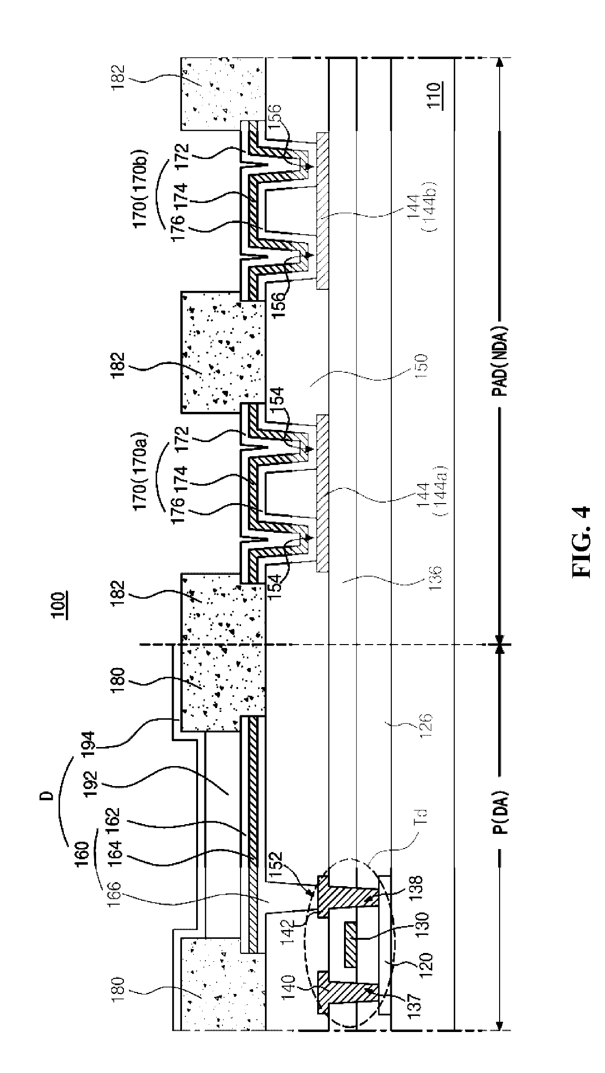
[0049]FIG. 4 is a schematic cross-sectional view of an electroluminescent display device according to the present disclosure.
[0050]In FIG. 4, the electroluminescent display device 100 includes a substrate 110, a light-emitting diode D, a pad 144, an auxiliary pad 170 connected to the pad 144, and an insulation pattern 182 disposed between adjacent auxiliary pads 170.
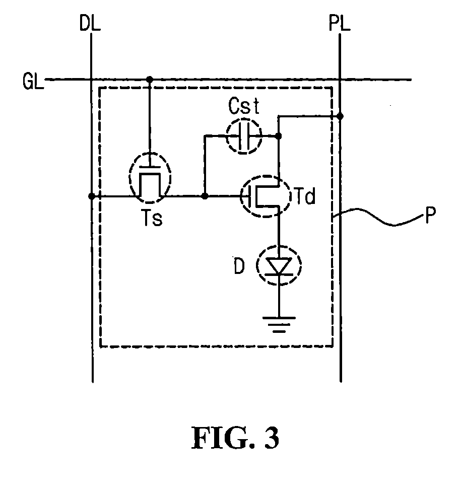
[0051]The pad 144 can be a data pad connected to a data line DL of FIG. 3. Alternatively, the pad 144 can be a gate pad, and in this instance, the gate pad can be formed of the same material and on the same layer as a gate line GL of FIG. 3.
[0052]The substrate 110 can be a glass substrate or a flexible plastic substrate. For example, the substrate 110 can be a polyimide substrate. A display area DA including a plurality of pixel regions P and a non-display area NDA disposed outside the display area DA and including a pad region PAD are defined on the substrate 110.
[0053]A driving thin film transistor Td is formed on the ...
second embodiment
[0091]In FIG. 5, the electroluminescent display device 200 according to the present disclosure includes a substrate 210, a light-emitting diode D, a pad 244, an auxiliary pad 270 connected to the pad 244, and an insulation pattern 282 disposed between adjacent auxiliary pads 270 and spaced apart from the auxiliary pads 270.
[0092]The pad 244 can be a data pad connected to a data line DL of FIG. 3. Alternatively, the pad 244 can be a gate pad, and in this instance, the gate pad can be formed of the same material and on the same layer as a gate line GL of FIG. 3.
[0093]A display area DA including a plurality of pixel regions P and a non-display area NDA disposed outside the display area DA and including a pad region PAD are defined on the substrate 210.
[0094]A driving thin film transistor Td is formed in the pixel region P of the display area DA on the substrate 210, and the pad 244 is formed in the pad region PAD of the non-display area NDA on the substrate 210. The driving thin film t...
third embodiment
[0112]In FIG. 6, the electroluminescent display device 300 according to the present disclosure includes a substrate 310, a light-emitting diode D, a pad 344, an auxiliary pad 370 connected to the pad 344, and an insulation pattern 382 disposed between adjacent auxiliary pads 370.
[0113]The pad 344 can be a data pad connected to a data line DL of FIG. 3. Alternatively, the pad 344 can be a gate pad, and in this instance, the gate pad can be formed of the same material and on the same layer as a gate line GL of FIG. 3.
[0114]A display area DA including a plurality of pixel regions P and a non-display area NDA disposed outside the display area DA and including a pad region PAD are defined on the substrate 310.
[0115]A driving thin film transistor Td is formed in the pixel region P of the display area DA on the substrate 310, and the pad 344 is formed in the pad region PAD of the non-display area NDA on the substrate 310. The driving thin film transistor Td can include a semiconductor laye...
PUM
Abstract
An electroluminescent display device can include a substrate having a display area and a pad region; a thin film transistor in the display area; first and second pads in the pad region; an insulating layer covering the thin film transistor and the first and second pads; first and second pad contact holes exposing the first and second pads, respectively; a light-emitting diode electrically connected to the thin film transistor and including first and second electrodes and a light-emitting layer interposed therebetween; and first and second auxiliary pads on the insulating layer, the first and second auxiliary pads being electrically connected to the first and second pads, respectively, in which each of the first electrode and the first and second auxiliary pads includes a first layer formed of a transparent conductive material and a second layer formed of a metallic material, and a surface length between the first and second auxiliary pads is greater than a distance between the first and second auxiliary pads.
Description
CROSS-REFERENCE TO RELATED APPLICATION[0001]The present application claims priority from and the benefit under 35 U.S.C § 119(a) of Korean Patent Application No. 10-2017-0180779 filed in the Republic of Korea on Dec. 27, 2017, which is hereby incorporated by reference in its entirety.BACKGROUND OF THE INVENTIONField of the Disclosure[0002]The present disclosure relates to an electroluminescent display device, and more particularly, to an electroluminescent display device capable of preventing an electrical short problem between pads.Discussion of the Related Art[0003]Among flat panel displays, electroluminescent display devices have wider viewing angles as compared with liquid crystal display devices because they are self-luminous. The electroluminescent display devices have a thin thickness and a light weight because they do not need a backlight and also have advantages in power consumption.[0004]The electroluminescent display devices are driven by a low voltage of direct current (...
Claims
Application Information
Patent Timeline
Application Date:The date an application was filed.
Publication Date:The date a patent or application was officially published.
First Publication Date:The earliest publication date of a patent with the same application number.
Issue Date:Publication date of the patent grant document.
PCT Entry Date:The Entry date of PCT National Phase.
Estimated Expiry Date:The statutory expiry date of a patent right according to the Patent Law, and it is the longest term of protection that the patent right can achieve without the termination of the patent right due to other reasons(Term extension factor has been taken into account ).
Invalid Date:Actual expiry date is based on effective date or publication date of legal transaction data of invalid patent.

