Stress isolation for silicon photonic applications

a silicon photonic and stress isolation technology, applied in the direction of instruments, optical elements, optical waveguide light guides, etc., can solve the problems of unwanted stress, damage to one or more photonic and/or electronic devices in the si-pic package, and damage to the si-pic packag

Active Publication Date: 2019-07-04
INTEL CORP
View PDF8 Cites 2 Cited by
  • Summary
  • Abstract
  • Description
  • Claims
  • Application Information

AI Technical Summary

Problems solved by technology

One problem that can affect an Si-PIC package is unwanted stress that is introduced into the package by one or more processes used to the form the package.
The stress may damage one or more photonic and / or electronic devices in the Si-PIC package.
This damage can cause the photonic and / or electronic device(s) to malfunction, result in destruction of the photonic device(s), or cause degradation of the photonic performance or targeted wavelength and / or decay the lifetimes. For example, an Si-PIC package may include: (i) a laser light source soldered onto a heat spreader; and (ii) the heat spreader soldered onto a heat sink.
The stress or strain applied to the laser may result in damaging the laser light source or shifting the wavelength of operation.
Local stresses may negatively affect one or more photonic devices of an Si-PIC package causing changes in refractive indices of the one or more photonic devices.
Such changes can result from temperature and / or pressure variations and each may affect the photonic device(s) performance.

Method used


Image

  • Stress isolation for silicon photonic applications
  • Stress isolation for silicon photonic applications
  • Stress isolation for silicon photonic applications

Examples


Embodiment Construction

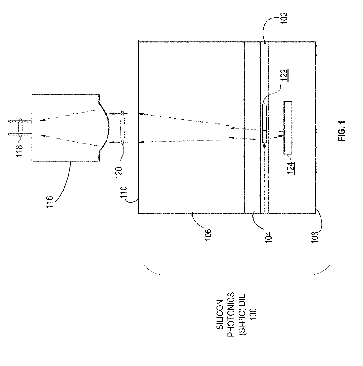
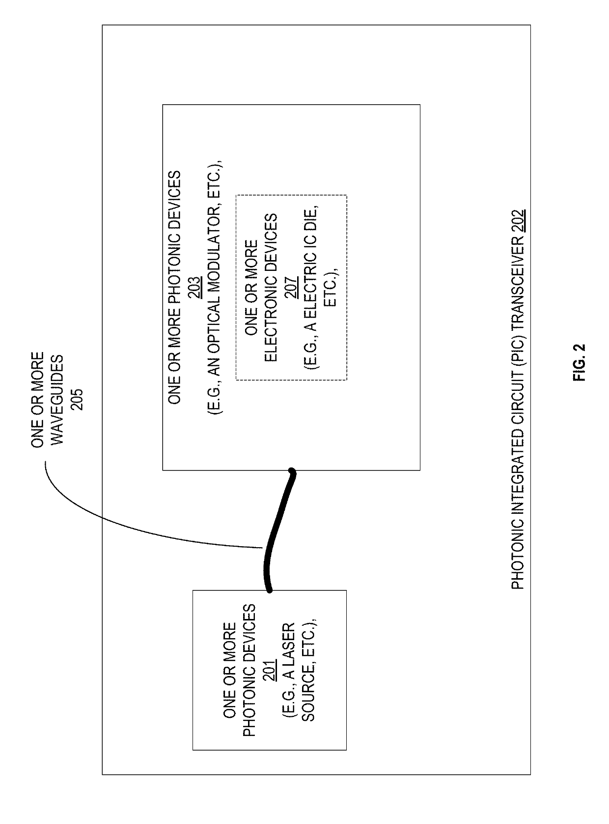
[0016]Embodiments described herein provide techniques of minimizing or eliminating stresses in Si-PICs or Si-PIC packages. For one embodiment, an Si-PIC or an Si-PIC package includes a stress minimization solution that assists with filtering out stresses by selectively isolating photonic and / or electronic devices. Examples of photonic devices include, but are not limited to, laser sources, laser amplifiers, optical modulators, and waveguides and photodetectors (e.g., as shown in FIG. 1, etc.). For one embodiment, an Si-PIC package includes a stress minimization solution that assists with isolating components in the Si-PIC package that are sources of stress. Examples of electronic devices include, but are not limited to, one or more of the following: (i) an electronic IC die, such as, a driver, clock data recovery re-timing chip, transimpedence amplifier, etc.; and (ii) an electronic IC package comprising at least one electronic IC die. For one embodiment, an Si-PIC package includes ...


PUM


Abstract

Techniques of minimizing or eliminating stresses in silicon photonic integrated circuits (Si-PICs) and in semiconductor packages having one or more Si-PICs (Si-PIC packages) are described. An Si-PIC or an Si-PIC package includes a stress minimization solution that assists with filtering out stresses by selectively isolating photonic and/or electronic devices, by isolating components or devices in an Si-PIC or an Si-PIC package that are sources of stress, or by isolating an Si-PIC in an Si-PIC package. The stress minimization solution may include strategically placed cavities and a stage that assist with minimizing or preventing transfer of stress to one or more photonic and/or electronic devices in an Si-PIC or an Si-PIC package.

Description

FIELD[0001]Embodiments generally relate to silicon photonic integrated circuits (Si-PICs) and semiconductor packages that include one or more Si-PICs (Si-PIC packages). More specifically, embodiments relate to techniques of minimizing or eliminating stresses in Si-PIC and Si-PIC packages.BACKGROUND INFORMATION[0002]Electronic systems that include one or more Si-PICs can exhibit relatively higher bandwidth data transmission rates over longer distances with relatively fewer copper interconnections than is possible with electronic devices that include electronic integrated circuits (electronic IC dies). This is because the data is converted from an electrical signal to an optical one and then transmitted through waveguides and fibers.[0003]An Si-PIC is an example of a semiconductor die that may be used in an electronic system, such as a switch or server. Si-PICs are capable of transmitting and receiving optical signals (e.g., pulses of light, etc.), which can be used to communicate dat...

Claims


Application Information

Patent Timeline
Patent Type & Authority Applications(United States)
IPC IPC(8): H01L23/498H01L21/48H01L23/00
CPCH01L23/49838H01L21/4803H01L24/16H01L2224/16225H01L2924/3511H01L2924/1515H01L2924/1015G02B6/122G02B6/12G02B6/13G02B2006/12061G02B2006/12085G02B2006/12166H01L2224/16227H01L2224/73204H01L2224/32225H01L2224/2919H01L2924/15159H01L24/29H01L24/32G02B6/4245G02B6/12004H01L23/13H01L2924/0665H01L2924/00
Inventor KUMAR, SIDDARTHLIFF, SHAWNA M.
Owner INTEL CORP
Why Eureka
Try Eureka