Structures and methods for electrically and mechanically linked monolithically integrated transistor and MEMS/NEMS devices

A device and mechanical technology, applied in the fields of electro-solid devices, semiconductor/solid-state device components, piezoelectric/electrostrictive/magnetostrictive devices, etc., can solve problems such as insufficient and incapable of reflecting the theme

Active Publication Date: 2013-12-04
CORNELL UNIVERSITY
View PDF27 Cites 2 Cited by
  • Summary
  • Abstract
  • Description
  • Claims
  • Application Information

AI Technical Summary

Problems solved by technology

For example, some or all of the publications discussed may not be sufficiently old in time, may not reflect subject matter developed sufficiently early in time, and / or may not be sufficiently enforceable to achieve patent law requirements. degree of prior art

Method used


Image

  • Structures and methods for electrically and mechanically linked monolithically integrated transistor and MEMS/NEMS devices
  • Structures and methods for electrically and mechanically linked monolithically integrated transistor and MEMS/NEMS devices
  • Structures and methods for electrically and mechanically linked monolithically integrated transistor and MEMS/NEMS devices

Examples


Embodiment Construction

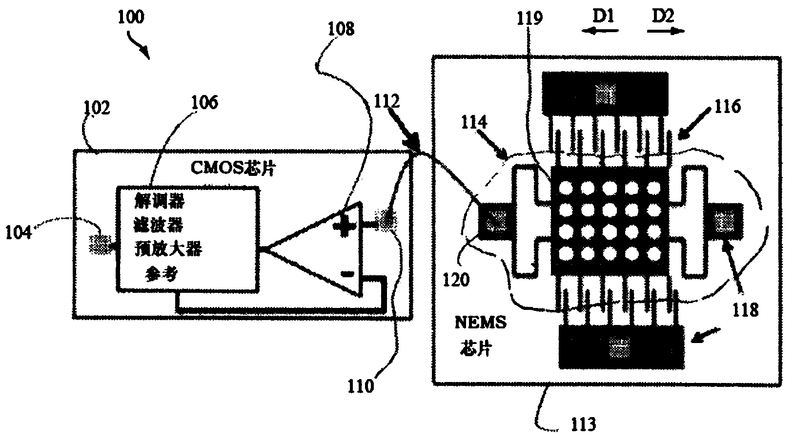
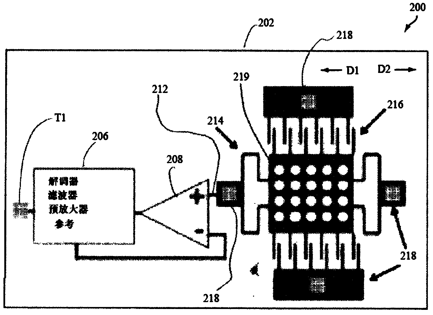
[0057] figure 2 A NEMS / MEMS device 200 is shown, which essentially consists of a single monolithically integrated chip 202 . In some embodiments, the NEMS / MEMS device may include additional control electronics, such as a processing network, on the second chip substrate. However, in device 200 , the NEMS / MEMS machinery and at least one transistor associated therewith are located on a single chip 202 . Such as figure 2 As shown, chip 202 includes: first terminal T1; demodulator / filter / preamplifier / reference module 206; amplifier 208; non-bonding path 212; fixed anchor structure 218; spring / mass subassembly 214; block 219; and finger structure 216.

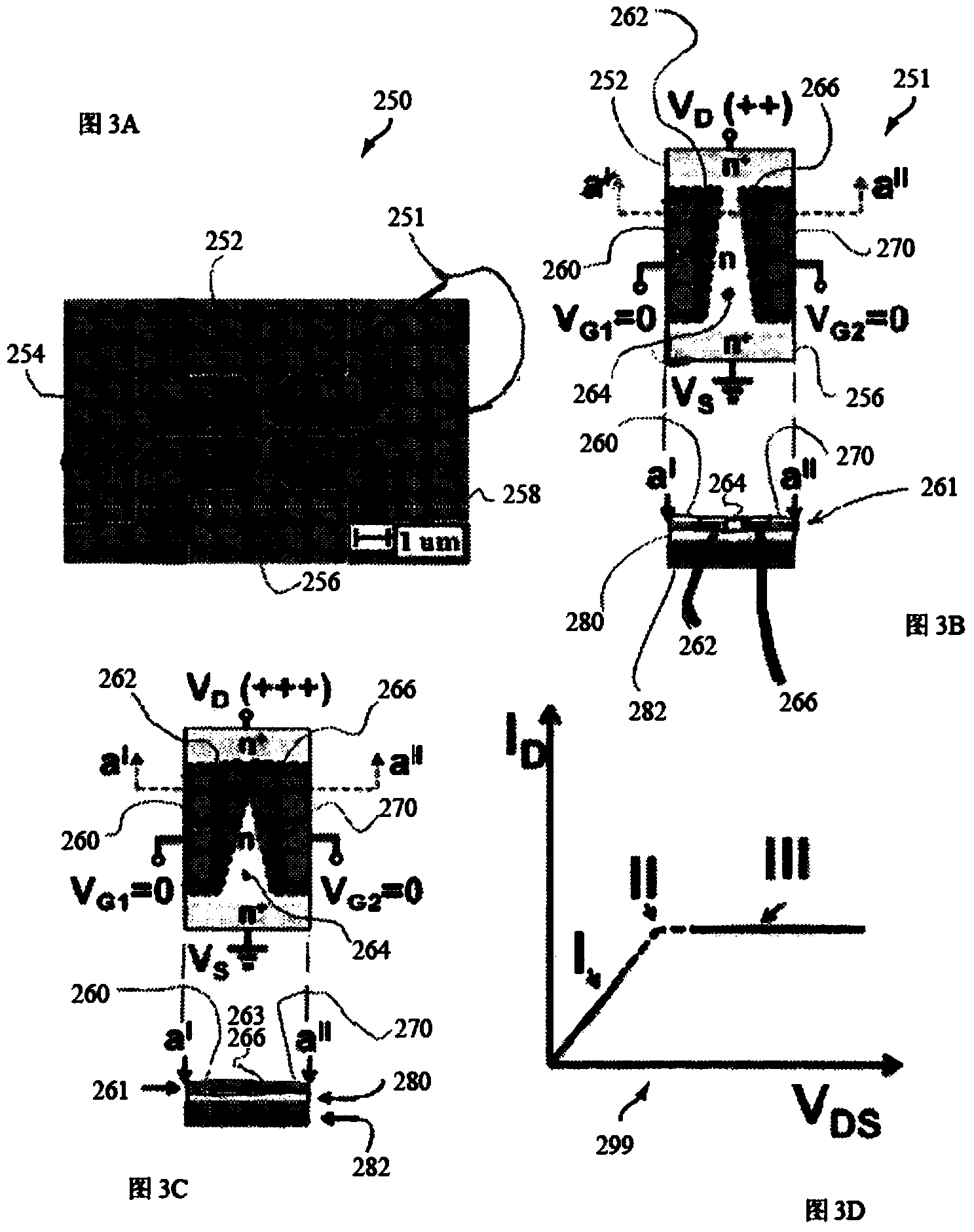
[0058] now refer to Figures 3A to 3D Modes of operation of NEMS / MEMS devices according to the present invention are discussed. Such as Figure 3A As shown, JFET 250 includes a drain region 252 ; a first gate region 254 ; a source region 256 ; a second gate region 258 and a channel region 251 . Such as Figure 3B and 3C As s...


PUM


Abstract

A device including a NEMS/MEMS machine(s) and associated electrical circuitry. The circuitry includes at least one transistor, preferably JFET, that is used to: (i) actuate the NEMS/MEMS machine; and/or (ii) receive feedback from the operation of the NEMS/MEMS machine The transistor (e.g., the JFET) and the NEMS/MEMS machine are monolithically integrated for enhanced signal transduction and signal processing. Monolithic integration is preferred to hybrid integration (e.g., integration using wire bonds, flip chip contact bonds or the like) due to reduce parasitics and mismatches. In one embodiment, the JFET is integrated directly into a MEMS machine, that is in the form of a SOI MEMS cantilever, to form an extra-tight integration between sensing and electronic integration. When a cantilever connected to the JFET is electrostatically actuated; its motion directly affects the current in the JFET through monolithically integrated conduction paths (e.g., traces, vias, etc.) In one embodiment, devices according to the present invention were realized in 2[mu]m thick SOI cross-wire beams, with a MoSi2 contact metallization for stress minimization and ohmic contact. In this embodiment, the pull-in voltage for the MEMS cantilever was 21V and the pinch-off voltage of the JFET was -19V.

Description

[0001] relevant application data [0002] This application claims priority to US Provisional Patent Application No. 61 / 418,467, filed December 1, 2010; all documents pertaining to said patent are hereby incorporated by reference in their entirety. [0003] Federally funded research or development [0004] The US Government has certain rights in this invention pursuant to Grant No. DMR0520404 awarded by NSF. technical field [0005] The present invention relates to JFETs and, in particular, to JFETs designed to facilitate the control of NEMS / MEMS level machinery (herein referred to as "NEMS / MEMS machinery", see also "NEMS / MEMS level" in the Definitions section) . The present invention also relates to devices comprising NEMS / MEMS machines and at least some circuitry for controlling the operation of the NEMS / MEMS machines (see Definitions section). These combinations of NEMS / MEMS mechanical hardware sets and at least a portion of its control circuitry (eg, JFETs) are sometimes...

Claims


Application Information

Patent Timeline
Patent Type & Authority Applications(China)
IPC IPC(8): H01L25/16B81B7/02
CPCH01L2924/0002B81C1/00246B81C2203/075H01L29/66893H01L25/16H01L29/735H01L29/66901H01L29/8086H01L29/42316H01L29/8126H01L2924/00
Inventor A·拉尔K·阿姆庞萨
Owner CORNELL UNIVERSITY
Why Eureka
Try Eureka