Eureka AIR delivers breakthrough ideas for toughest innovation challenges, trusted by R&D personnel around the world.

Resistorless power amplifier

Active Publication Date: 2019-08-08
ADVANCED SEMICON ENG INC
View PDF6 Cites 0 Cited by
  • Summary
  • Abstract
  • Description
  • Claims
  • Application Information

AI Technical Summary

Benefits of technology

The present patent describes different configurations of power amplifier circuits and a wireless communication system that use these circuits. These circuits have a current source, a power control circuit, a current mirror, and an output circuit, which work together to amplify signals in a controlled and efficient way. The circuits have been designed to improve the performance of wireless communication systems and provide better overall amplification of signals. The technical effects of the patent include improved signal amplification, increased efficiency, and better performance of wireless communication systems.

Problems solved by technology

However, the large resistors may increase a chip / die area, which can hinder miniaturization of the chip / die.

Method used


Image

  • Resistorless power amplifier
  • Resistorless power amplifier
  • Resistorless power amplifier

Examples


Embodiment Construction

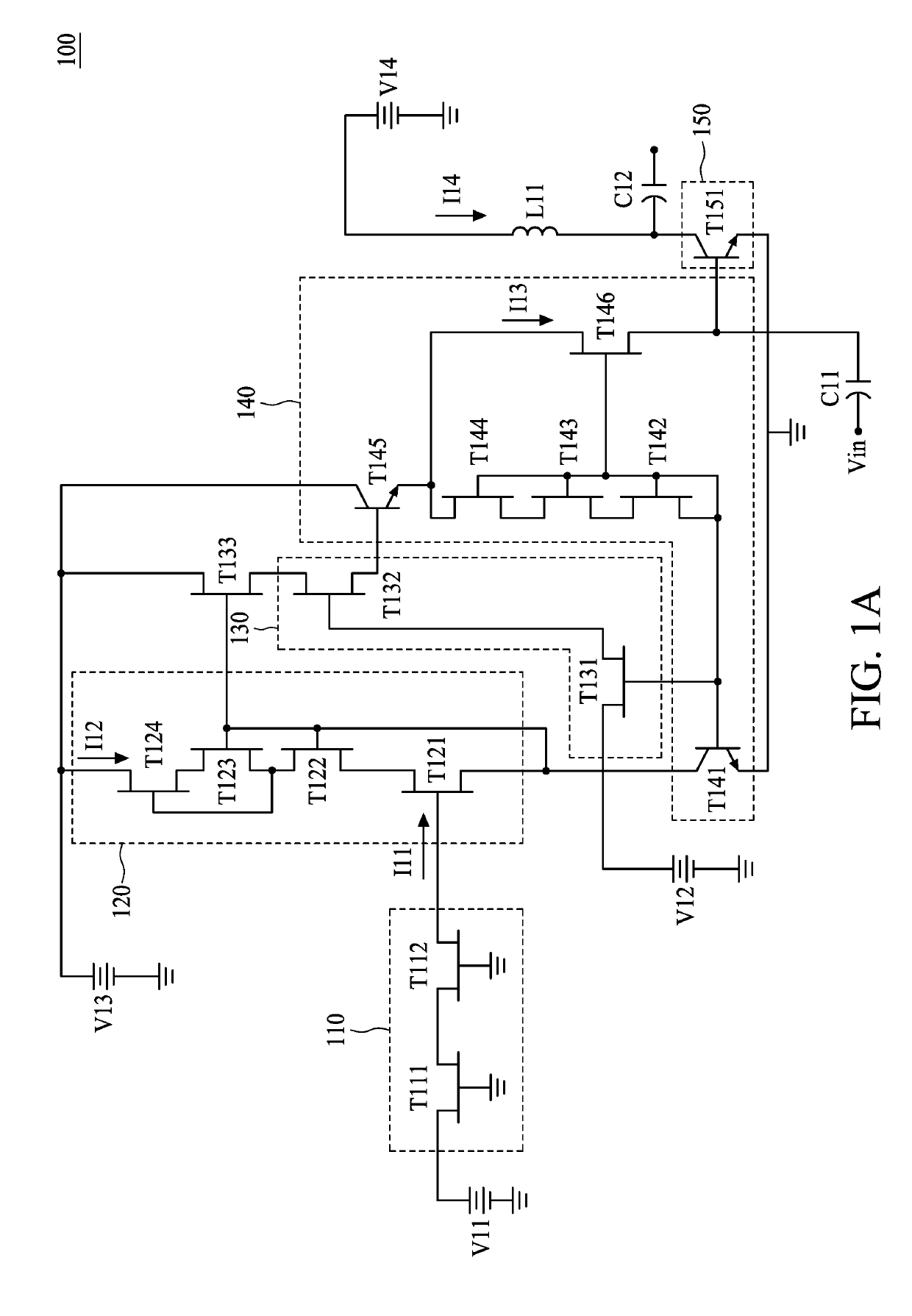
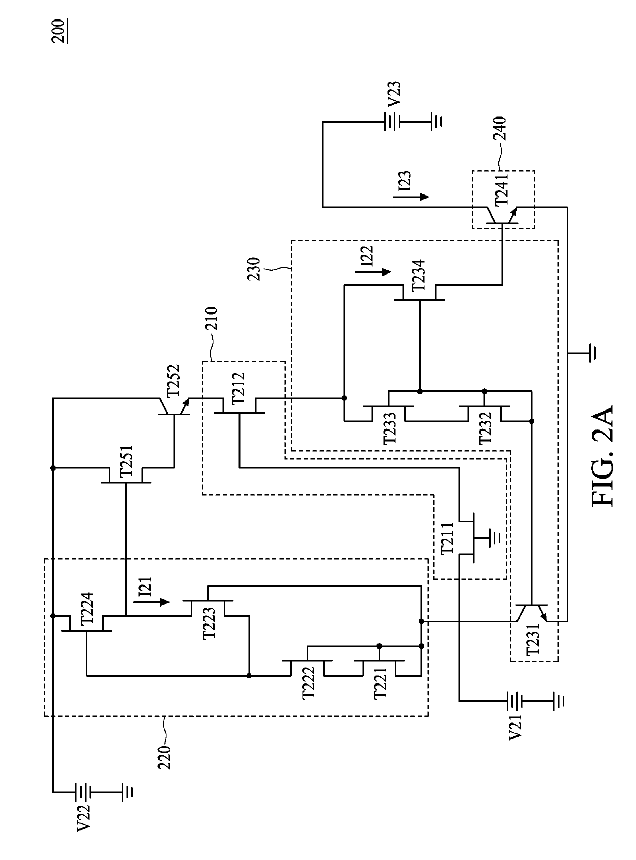
[0014]Although described with particular reference to a portable transceiver, the circuit and method for biasing a gallium arsenide (GaAs) power amplifier (also referred to as the GaAs bias circuit) can be implemented in any GaAs device in which it is desirable to provide a bias current and voltage. Furthermore, the circuitry described below can be fabricated using an integrated bipolar-field effect transistor (BIFET) process utilizing a lower turn-on voltage of field effect transistors. Furthermore, in particular embodiments, the transistors described below include bipolar junction transistors (referred to as a BJT), which includes heterojunction bipolar junction transistors (referred to as an HBT) and field effect transistors (referred to as a FET) or pseudomorphic high-electron mobility transistors (referred to as a pHEMT) that are fabricated using what is referred to as the BIFET or BiHEMT process.

[0015]As used herein, reference to a gate, source, drain, or other component of a ...


PUM


Abstract

The present disclosure relates to a power amplifier circuit including a current source, a power control circuit, a current mirror and an output circuit. The current source circuit includes a first transistor and a second transistor. A source of the first transistor is connected to a drain of the second transistor and a gate of the first transistor is connected to a source with the second transistor. The power control circuit is connected to a gate of the second transistor. The current mirror circuit is connected to the gate of the first transistor and a source of the second transistor. The output circuit is connected to the current mirror circuit.

Description

BACKGROUND1. Technical Field[0001]The present disclosure relates to a power amplifier, and more particularly, to a bias circuit for a power amplifier.2. Description of the Related Art[0002]A power amplifier is a circuit in a wireless transceiver for amplifying a signal to be transmitted. The power amplifier can be powered by a power source circuit, such as a current source (or a current sink) connected with a current mirror. When the power amplifier is used for mobile devices (such as a cell phone, a tablet or a notebook), it may be desirable to have the power consumption of the power amplifier and the power source circuit be relatively low. In order to precisely control or reduce the current applied to the power amplifier, relative large resistors (e.g. in a range of kilo-ohms (k ohms) to mega-ohms (M ohm)) can be used. However, the large resistors may increase a chip / die area, which can hinder miniaturization of the chip / die.SUMMARY[0003]In accordance with an aspect of the present...

Claims


Application Information

Patent Timeline
IPC IPC(8): H03F1/02H03F3/19H03F3/21
CPCH03F1/0205H03F3/19H03F3/21H03F2200/451H04B1/04
Inventor DING, JAW-MING
Owner ADVANCED SEMICON ENG INC
Why Eureka
Eureka Blog
Learn More