Element unit

a technology of elements and components, applied in the field of elements, can solve the problems of increasing the total stray inductance of the series circuit, and achieve the effects of reducing stray inductance, increasing length, and efficiently disposing

Active Publication Date: 2019-08-15
HONDA MOTOR CO LTD
View PDF1 Cites 0 Cited by
  • Summary
  • Abstract
  • Description
  • Claims
  • Application Information

AI Technical Summary

Benefits of technology

[0014]According to the aspect (1), since the positive electrode side conductor and the negative electrode side conductor extend to face each other, flowing directions of mutual currents are opposite to each other, and it is possible to reduce a stray inductance by a mutual magnetic flux offsetting action. In addition, a length of each of the positive electrode side conductor and the negative electrode side conductor is restrained from increasing at a portion not facing each other. That is, the stray inductance of the positive electrode side conductor and the negative electrode side conductor can reduce the stray inductance due to the mutual magnetic flux offsetting action and the restraining of the increase in the length.
[0015]In the case of the aspect (2), the second conductor, the low side arm element, the negative electrode side conductor, the positive electrode side conductor, the high side arm element, and the first conductor can be efficiently disposed while making electrical connection, and thus the increase in the stray inductance can be suppressed.
[0016]In the case of the aspect (3), since the high side arm element, the conductor set, and the low side arm element are disposed at positions which overlap each other, it is possible to restrain an increase in a planar size (area) of the element unit.
[0017]In the case of the aspect (4), since the high side arm element and the low side arm element are disposed at positions not overlapping each other, mutual thermal interference can be suppressed. For example, it is possible to suppress heat generation of any one of the high side arm element and the low side arm element from being transmitted to other elements.
[0018]In the case of the aspect (5), since the input / output conductor is disposed at a position which does not interfere with the positive electrode side conductor and the negative electrode side conductor, the input / output conductor can be easily drawn out from the element unit.
[0019]In the case of the aspect (6), each of the high side arm element and the low side arm element is disposed at the position not overlapping the insulating member which insulates the positive electrode side conductor and the negative electrode side conductor when seen in the predetermined direction and can be cooled from both sides in the predetermined direction, thus an increase in thermal resistance can be suppressed, and the cooling performance can be improved. Also, the increase in the stray inductance can be suppressed by restraining an increase in a thickness of the element unit in the predetermined direction and disposing it in a compact manner.

Problems solved by technology

However, when the positive electrode side bus bar and the negative electrode side bus bar are drawn out from positions away from each other in the arrangement direction of the first semiconductor element and the second semiconductor element like the semiconductor modules according to the above-described related art, there arises a problem that the total stray inductance of the series circuit increases due to a self-inductance of each of the bus bars.

Method used


Image

  • Element unit
  • Element unit
  • Element unit

Examples


first example

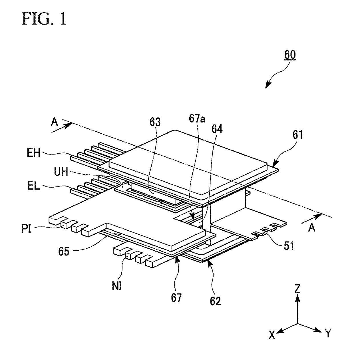
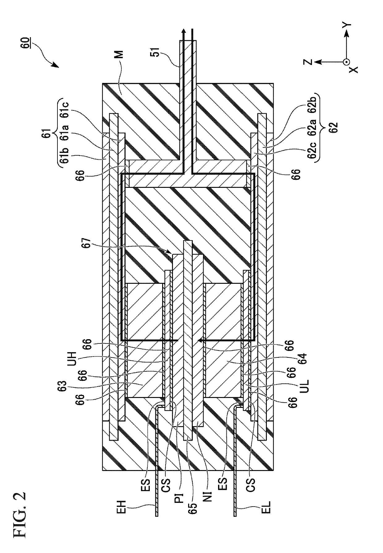
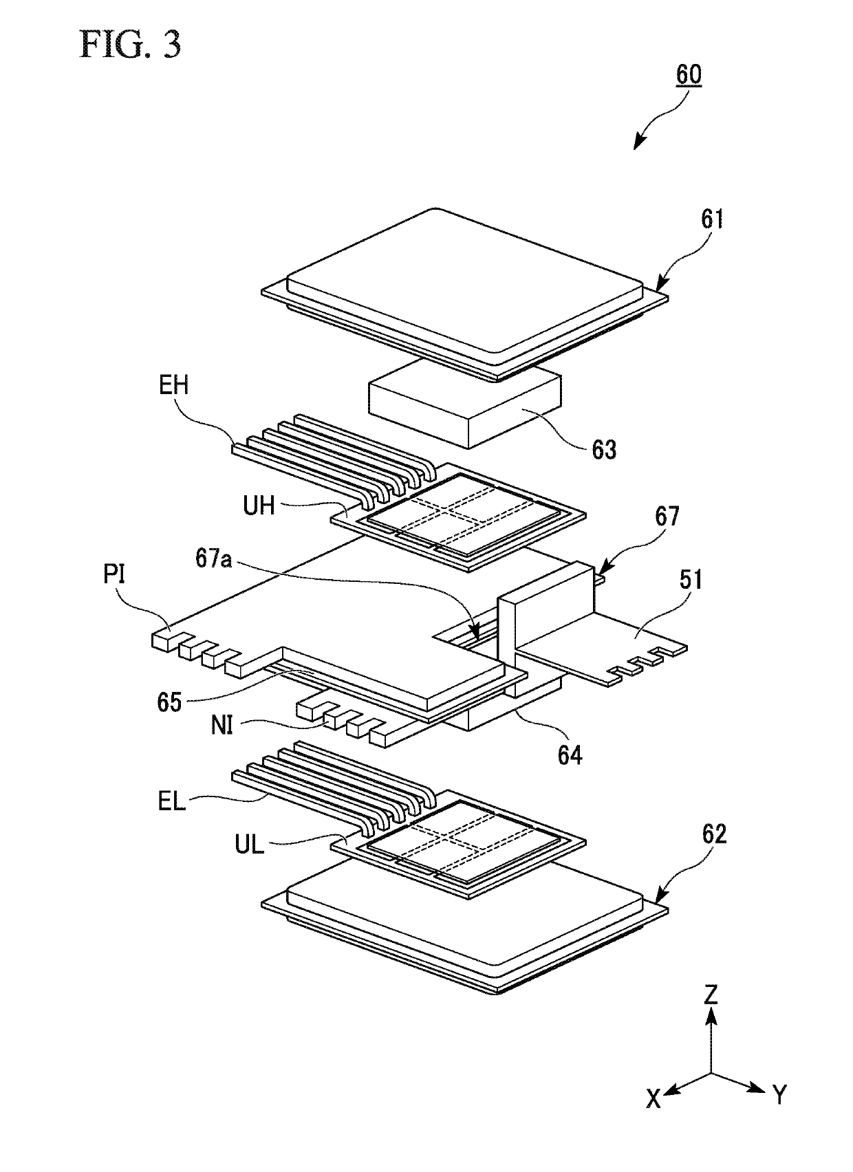
[0040]FIG. 1 is a perspective view schematically showing a constitution of an element unit 60 according to a first example of an embodiment of the present invention. FIG. 2 is a diagram showing a current path in a cross-sectional view taken along a Y-Z plane at a position of line A-A shown in FIG. 1. FIG. 3 is an exploded perspective view schematically showing the constitution of the element unit 60 according to the first example of the embodiment of the present invention. FIG. 4 is a diagram showing a constitution of part of a vehicle 10 equipped with a power conversion device 1 including the element unit 60 according to the embodiment of the present invention.

[0041]As shown in FIG. 4, the vehicle 10 includes a battery 11 (BATT), a first motor 12 (MOT) for traveling and driving, and a second motor 13 (GEN) for power generation in addition to the power conversion device 1.

[0042]The battery 11 includes a battery case and a plurality of battery modules accommodated in the battery case...

second example

[0101]FIG. 7 is a perspective view schematically showing a constitution of an element unit 70 according to a second example of the embodiment of the present invention. FIG. 8 is a cross-sectional view taken along the Y-Z plane at a position of line B-B shown in FIG. 7. FIG. 9 is a diagram showing a current path in an exploded perspective view schematically showing the constitution of the element unit according to the second example of the embodiment of the present invention.

[0102]In the following, the constitution of the element unit 70 including the high side arm U-phase transistor UH and the low side arm U phase transistor UL in the U-phase of the first power conversion circuit unit 31 will be described as a representative example of the element unit 70 according to the second example, like the first example.

[0103]The element unit 70 includes a resin molded body M, high side arm and low side arm U-phase transistors UH and UL, a high side arm gate electrode EH and a low side arm ga...

third example

[0131]FIG. 10 is a perspective view schematically showing a constitution of an element unit 80 according to a third example of the embodiment of the present invention. FIG. 11 is a cross-sectional view taken along the Y-Z plane at a position of line C-C shown in FIG. 10. FIG. 12 is a cross-sectional view taken along the Y-Z plane at a position of line D-D shown in FIG. 10. FIG. 13 is a diagram showing a current path on a positive electrode side in an exploded perspective view schematically showing the constitution of the element unit according to the third example of the embodiment of the present invention. FIG. 14 is a diagram showing a current path on a negative electrode side in the exploded perspective view schematically showing the constitution of the element unit according to the third example of the embodiment of the present invention.

[0132]In the following, the constitution of the element unit 80 including the high side arm U-phase transistor UH and the low side arm U-phase ...


PUM


Abstract

There is provided an element unit including high side arm and low side arm transistors, a conductor set formed by disposing a positive bus bar and a negative bus bar to face each other while spaced apart in a Z axis direction, and a first bus bar. The first bus bar extends in the Z axis direction between a first insulating substrate and a second insulating substrate and is electrically connected to copper plates of the first insulating substrate and the second insulating substrate.

Description

CROSS-REFERENCE TO RELATED APPLICATION[0001]Priority is claimed on Japanese Patent Application No. 2018-022545, filed Feb. 9, 2018, the content of which is incorporated herein by reference.BACKGROUND OF THE INVENTIONField of the Invention[0002]The present invention relates to an element unit.Description of Related Art[0003]Conventionally, a power control unit including a plurality of semiconductor modules stacked and disposed in a first direction (a stacking direction) is known (for example, refer to Japanese Unexamined Patent Application, First Publication No. 2012-235081). Each of the semiconductor modules of the power control unit includes a first semiconductor element and a second semiconductor element arranged and disposed in a second direction (an arrangement direction) orthogonal to the first direction. The first semiconductor element and the second semiconductor element are disposed so that surfaces (for example, active surfaces on which a gate electrode is provided) thereof...

Claims


Application Information

Patent Timeline
Patent Type & Authority Applications(United States)
IPC IPC(8): H02M7/00H05K7/02
CPCH02M7/003H05K7/023H01L25/16H01L23/3121H01L23/49833H01L23/49548H01L23/49575H02M7/53875H02M3/158H01L2924/181H01L2224/32225H01L2224/33181H02M1/008H02M1/007H05K7/14329H01L2924/00012
Inventor UNEME, TAKAHIRO
Owner HONDA MOTOR CO LTD
Why Eureka
Try Eureka