Alloy metal foil for use as deposition mask, deposition mask, methods of preparing the same, and method of manufacturing organic light-emitting device using the same
- Summary
- Abstract
- Description
- Claims
- Application Information
AI Technical Summary
Benefits of technology
Problems solved by technology
Method used
Image

Examples
Embodiment Construction
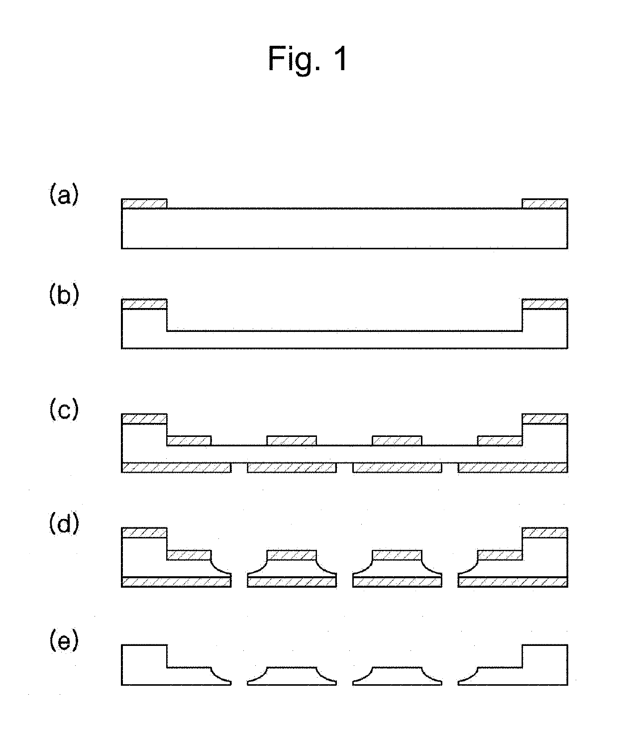
[0032]Recently, as pixel refinement has become necessary, when forming through-hole patterns with a relatively thick metal foil of about 50-100 μm, this excessive thickness of the metal foil may give rise technical difficulties in obtaining patterns of high resolution, and for example, interference between patterns may arise during an etching process, thus hindering accurate pattern formation. Meanwhile, a relatively thin metal foil of about 20 μm or less, when used to form through-hole patterns, may degrade strength and cause substrate deformation and the like in producing a deposition mask, and are often accompanied by working and handling difficulties.
[0033]In this context, the present disclosure provides a method of producing a deposition mask in which patterns can be formed accurately while using a relatively thick metal foil; and a deposition mask prepared thereby.
[0034]The present disclosure uses a Fe—Ni alloy as a deposition mask, and any material that contains 34-46 wt % of...
PUM
| Property | Measurement | Unit |
|---|---|---|
| Fraction | aaaaa | aaaaa |
| Fraction | aaaaa | aaaaa |
| Fraction | aaaaa | aaaaa |
Abstract
Description
Claims
Application Information