Lighting device using ambipolar transistors

a technology of ambipolar transistors and lighting devices, which is applied in the direction of semiconductor devices for light sources, lighting and heating apparatus, electroluminescent light sources, etc., can solve the problems of reducing the lifespan of electronic devices, spark generation, and the size of semiconductor devices

Inactive Publication Date: 2019-09-12
OH TERESA
View PDF0 Cites 0 Cited by
  • Summary
  • Abstract
  • Description
  • Claims
  • Application Information

AI Technical Summary

Problems solved by technology

However, there can actually be problems such as short circuit or over-discharge of a battery, overheating of an LED lamp, generation of sparks, and reduction in lifespan of electronic devices due to electrical instability.
These problems can be caused by various factors, but are mainly caused by noise and leakage current.
In addition, reduction in size of semiconductor devices provides a problem relating to SiO2 thin film dielectrics, such as increase in power consumption due to current leakage, signal interference, and the like, due to limitations of silicon semiconductor technology.
Moreover, current leakage provides serious problems in applications including various electronic sensors using semiconductors, displays, smart phones, and batteries.
However, the LEDs create much heat caused by accompanied resistors, for this reason lighting devices with LEDs need to be equipped with heat sinks.

Method used


Image

  • Lighting device using ambipolar transistors
  • Lighting device using ambipolar transistors
  • Lighting device using ambipolar transistors

Examples


first embodiment

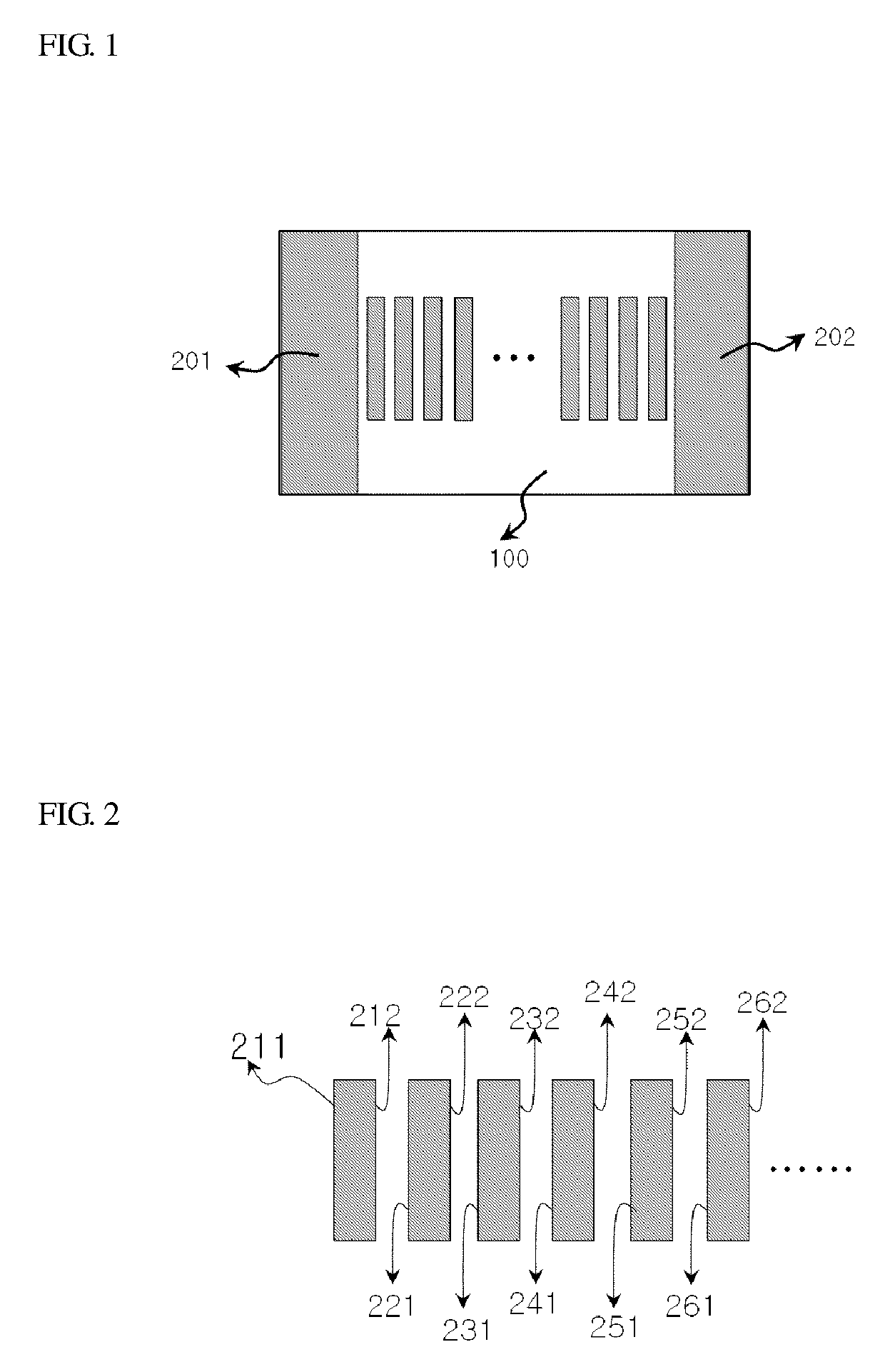
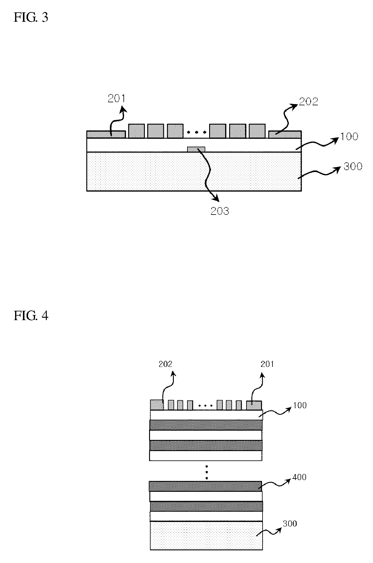
[0054]FIG. 1 is a top view of a series pattern diffusion current transistor according to the present invention, FIG. 2 is a view of a source-drain terminal pattern of the series pattern diffusion current transistor of FIG. 1, and FIG. 3 is a sectional view of the series pattern diffusion current transistor of FIG. 1.

[0055]Referring to FIGS. 1 to 3, an ambipolar transistor using diffusion current according to a first embodiment of the present invention includes: a gate 203 formed on a substrate 300; a gate insulating film 100 formed on the substrate 300 and the gate 203 and formed of a SiOC thin film; and a source portion and a drain portion formed on the gate insulating layer 100 and spaced apart from each other.

[0056]In addition, when drain and source signal lines are disposed on the gate insulating film 100, in order to amplify electrical signals (voltage) while increasing sensitivity, the source portion and the drain portion may include: a main source terminal 202 and a main drai...

second embodiment

[0062]An ambipolar transistor using diffusion current according to the present invention includes a gate 203 connected to a substrate 300, an interlayer electrode 400 formed on the substrate, an SiOC insulating film 100 formed on the interlayer electrode 400, and a source portion and a drain portion formed on the interlayer electrode and spaced apart from each other, wherein the interlayer electrode and the SiOC insulating film 100 include a plurality of interlayer electrodes and a plurality of SiOC insulating films alternately stacked one above another, respectively.

[0063]In addition, the source portion and the drain portion include: a main source terminal 202 and a main drain terminal 201 disposed at right and left sides of the SiOC insulating film 100, respectively; and a plurality of source sub-terminals and a plurality of drain sub-terminals, respectively, wherein the plurality of source sub-terminals 212, 222, 232, . . . and the plurality of drain sub-terminals 211, 221, 231, ...

third embodiment

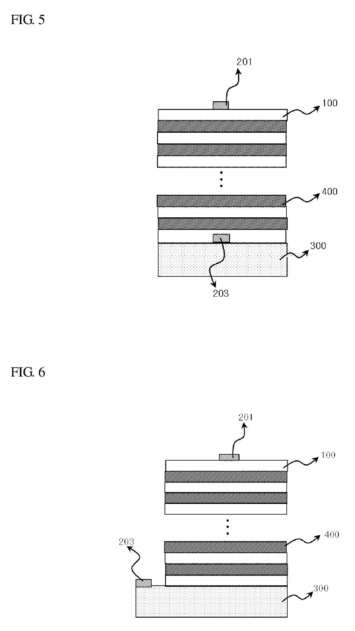
[0065]FIG. 5 is a sectional view of a series pattern diffusion current transistor according to the present invention. In this embodiment, the gate is formed in the SiOC insulating film 100 on the substrate.


PUM


Abstract

Disclosed are a light device using an ambipolar transistor, which comprises an LED connected to a drain electrode; a power source connected to the LED; a source electrode connected to the power source; and a gate electrode connected to both the LED and the drain electrode, wherein diffusion current between the source electrode and the drain electrode allows reception of electronic signal. The ambipolar transistor includes: a substrate; a gate formed on the substrate; a gate insulating film formed of an SiOC thin film and disposed on the substrate and the gate; and a source portion and a drain portion formed on the gate insulating film and spaced apart from each other, wherein the source portion and the drain portion comprise: a main source terminal and a main drain terminal disposed on the gate insulating film at right and left sides of the gate, respectively; and a plurality of source sub-terminals and a plurality of drain sub-terminals alternately arranged between the main source terminal and the main drain terminal, respectively.

Description

TECHNICAL FIELD[0001]The present invention relates to a lighting device using ambipolar transistors and, and more particularly, to a lighting device using LED which creates heat caused by accompanied resistors but was cancelled its heat via an ambipolar transistor, which can prevent current leakage using diffusion current having negative resistance characteristics due to a potential barrier caused by dielectrics, and can block leakage current in a lighting device.BACKGROUND[0002]Recently, an electric vehicle market has been gradually expanded. The life of a battery is closely related to the charging method and the discharging phenomenon and thus can be prolonged by removing leakage current.[0003]In an electric vehicle composed of various electronic devices, a leakage current cut-off sensor is an essential component. However, there can actually be problems such as short circuit or over-discharge of a battery, overheating of an LED lamp, generation of sparks, and reduction in lifespan...

Claims


Application Information

Patent Timeline
Patent Type & Authority Applications(United States)
IPC IPC(8): H05B33/08H05B37/02H05B33/06H05B44/00
CPCH05B33/06H05B33/0803H05B37/02H02M1/08H05B45/30H01L29/4234H01L21/823462H01L21/28185H01L21/02126H01L27/15F21K9/20F21Y2115/10
Inventor OH, TERESA
Owner OH TERESA
Why Eureka
Try Eureka