
Super-junction corner and termination structure with improved breakdown and robustness

a technology of junction corners and termination structures, applied in the direction of semiconductor devices, basic electric elements, electrical appliances, etc., can solve the problems of less robust devices, reduced breakdown voltage (bv) of semiconductor devices, and more difficult to achieve charge balan

Active Publication Date: 2019-10-03
ALPHA & OMEGA SEMICON CAYMAN
View PDF2 Cites 0 Cited by
  • Summary
  • Abstract
  • Description
  • Claims
  • Application Information

AI Technical Summary

Benefits of technology

The patent describes a power semiconductor device with improved breakdown voltage and better manufacturing yield. This is achieved by incorporating superjunction structures with slanted sidewalls where the grading of the superjunction columns in the termination region is reduced compared to the active cell region. The breakdown voltage of the termination region is increased while the breakdown characteristic of the device is determined by the breakdown voltage of the core region. Overall, this results in a more robust device with improved reliability and durability.

Problems solved by technology

However, at the edge termination regions and the corner regions, it is more difficult to achieve charge balance.
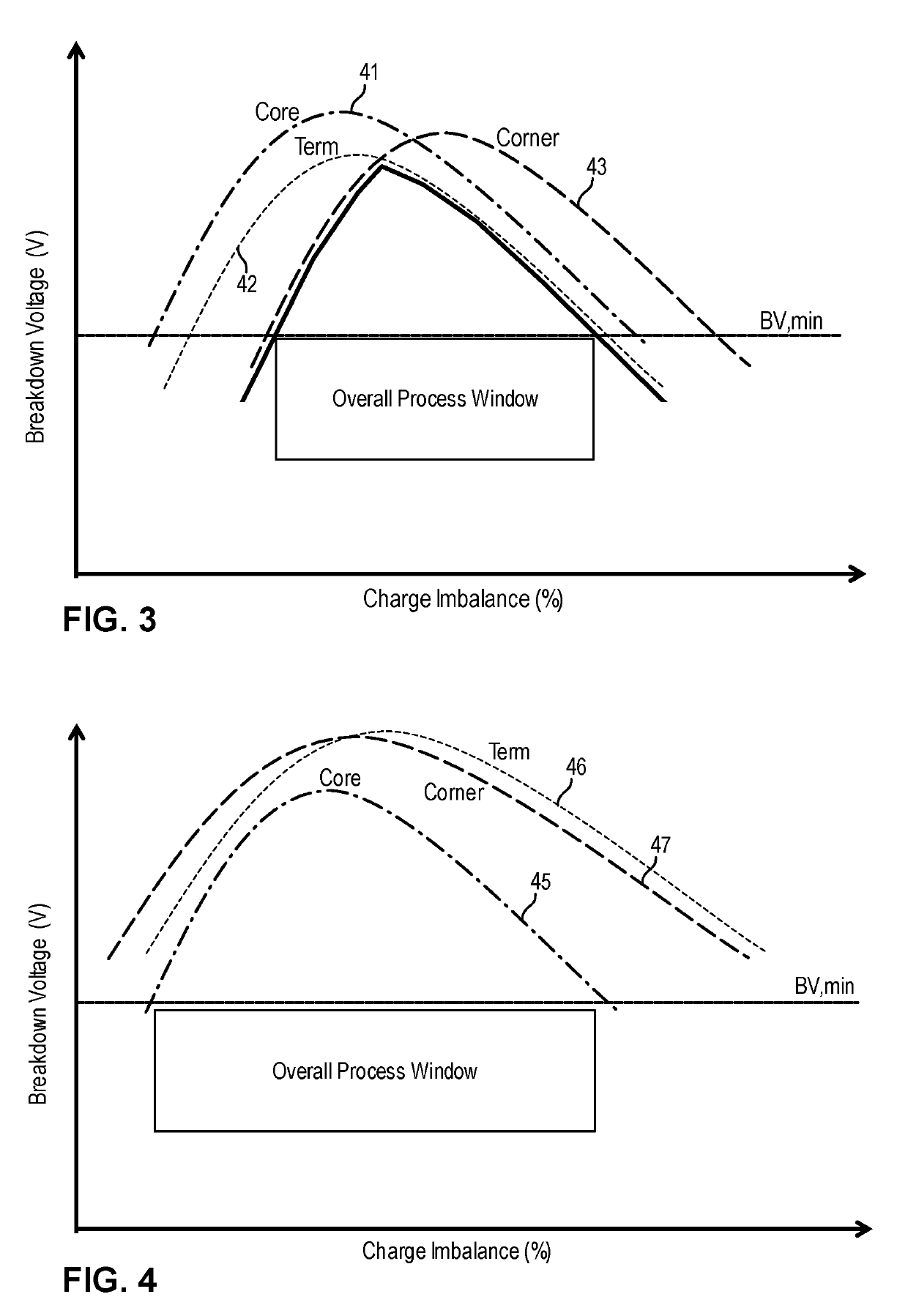
When charge balance is not maintained, the breakdown voltage (BV) of the semiconductor device decreases and the device becomes less robust.
Maintaining charge balance in the termination region at the corners or edges of the power semiconductor device remains challenging.

Method used


Image

  • Super-junction corner and termination structure with improved breakdown and robustness
  • Super-junction corner and termination structure with improved breakdown and robustness
  • Super-junction corner and termination structure with improved breakdown and robustness

Examples


Embodiment Construction

[0019]The invention can be implemented in numerous ways, including as a process; an apparatus; a system; and / or a composition of matter. In this specification, these implementations, or any other form that the invention may take, may be referred to as techniques. In general, the order of the steps of disclosed processes may be altered within the scope of the invention.

[0020]A detailed description of one or more embodiments of the invention is provided below along with accompanying figures that illustrate the principles of the invention. The invention is described in connection with such embodiments, but the invention is not limited to any embodiment. The scope of the invention is limited only by the claims and the invention encompasses numerous alternatives, modifications and equivalents. Numerous specific details are set forth in the following description in order to provide a thorough understanding of the invention. These details are provided for the purpose of example and the inv...


PUM


Abstract

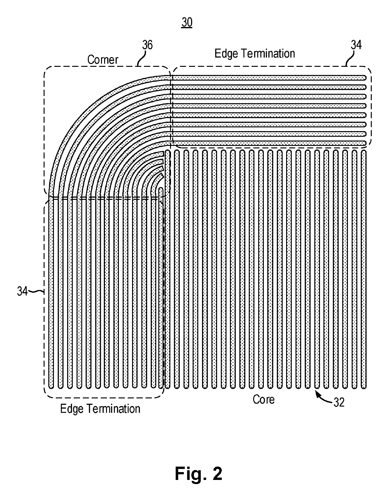
A superjunction power semiconductor device includes a termination region with superjunction structures having higher breakdown voltage than the breakdown voltage of the active cell region. In one embodiment, the termination region includes superjunction structures having lower column charge as compared to the superjunction structures formed in the active cell region. In other embodiments, a superjunction power semiconductor device incorporating superjunction structures with slanted sidewalls where the grading of the superjunction columns in the termination region is reduced as compared to the column grading in the active cell region. The power semiconductor device is made more robust by ensuring any breakdown occurs in the core region as opposed to the termination region. Furthermore, the manufacturing process window for the power semiconductor device is enhanced to improve the manufacturing yield of the power semiconductor device.

Description

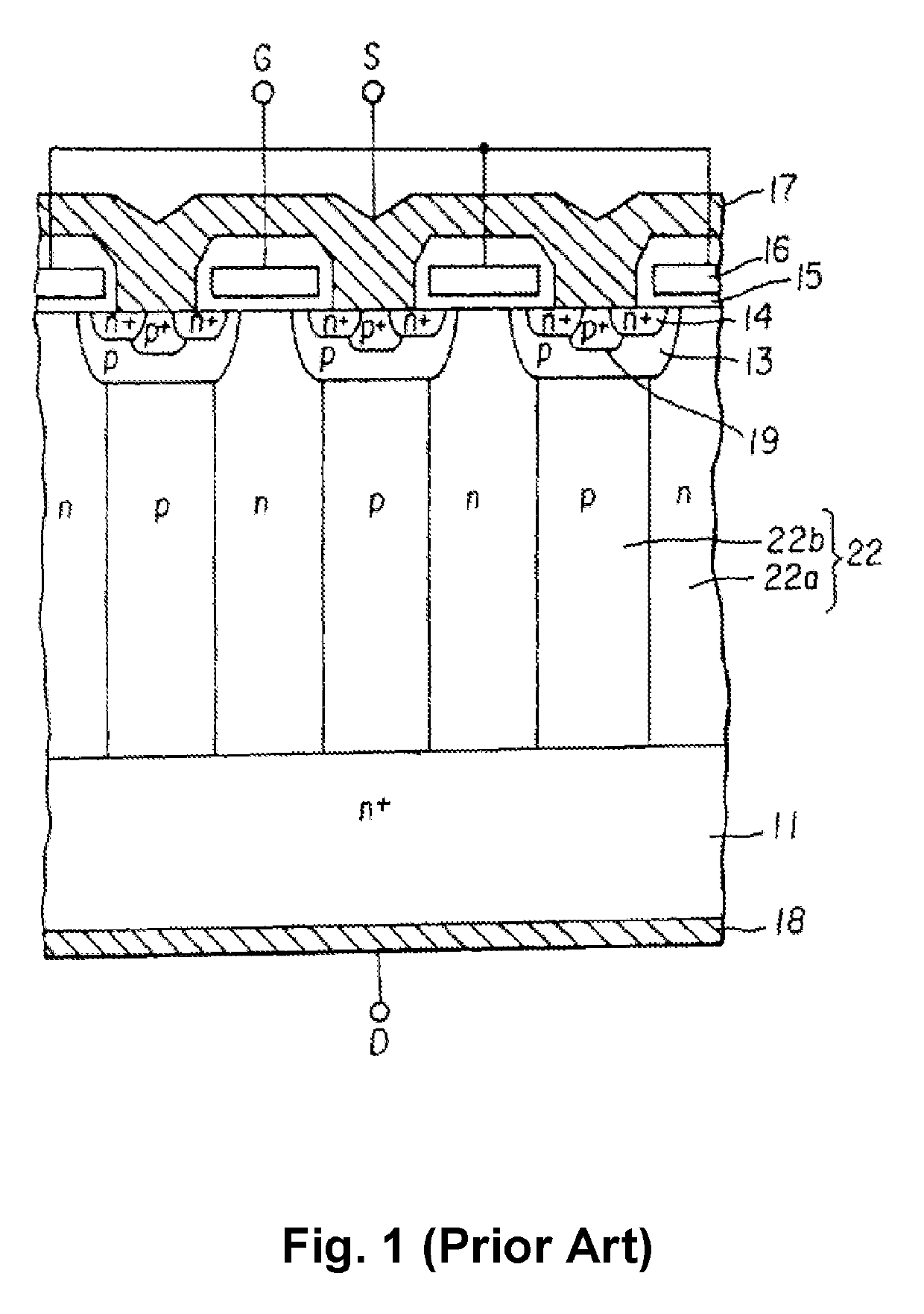
FIELD OF THE INVENTION[0001]The invention relates to power semiconductor devices and, in particular, to corner and termination structures for power semiconductor devices incorporating superjunction structures.BACKGROUND OF THE INVENTION[0002]Semiconductor devices incorporating superjunction structure to achieve improved electrical characteristics are known. For example, metal oxide semiconductor field effect transistor (MOSFET) devices can be incorporated with vertical or horizontal superjunction structure to optimize the on-resistance and the breakdown voltage characteristics of the transistor. As an example, Fujihira describes configurations of the lateral and vertical superjunction devices in the paper entitled “Theory of Semiconductor Superjunction Devices” (Japan Journal of Applied Physics Vol. 36, October 1997, pp. 6254-6262).[0003]More specifically, superjunction transistors provide a way to achieve low on-resistance (Rds-on), while maintaining a high off-state breakdown volt...

Claims


Application Information

Patent Timeline
Patent Type & Authority Applications(United States)
IPC IPC(8): H01L29/15H01L29/06H01L29/08
CPCH01L29/0696H01L29/0619H01L29/0878H01L29/0886H01L29/158H01L29/157H01L29/0684H01L29/0611H01L29/0603H01L29/7802H01L29/0634H01L29/7811H01L29/66712
Inventor BOBDE, MADHURPADMANABHAN, KARTHIKGUAN, LINGPENG
Owner ALPHA & OMEGA SEMICON CAYMAN
Learn More