Photodetector including a geiger mode avalanche photodiode and an integrated resistor and related manufacturing method

a photodiode and photodiode technology, applied in the field of photodetectors, can solve the problems of reducing the possibility of miniaturization, increasing complexity and costs, and no longer detecting photons with spads

Active Publication Date: 2019-10-17
STMICROELECTRONICS SRL
View PDF0 Cites 3 Cited by
  • Summary
  • Abstract
  • Description
  • Claims
  • Application Information

AI Technical Summary

Problems solved by technology

Consequently, once the avalanche-ionization process has been triggered, the SPAD is no longer able to detect photons, with the consequence that, in the absence of appropriate remedies, the SPAD manages to detect arrival of a first...

Method used


Image

  • Photodetector including a geiger mode avalanche photodiode and an integrated resistor and related manufacturing method
  • Photodetector including a geiger mode avalanche photodiode and an integrated resistor and related manufacturing method
  • Photodetector including a geiger mode avalanche photodiode and an integrated resistor and related manufacturing method

Examples


Embodiment Construction

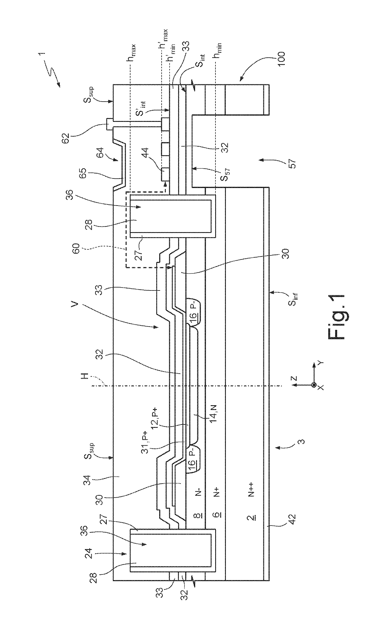
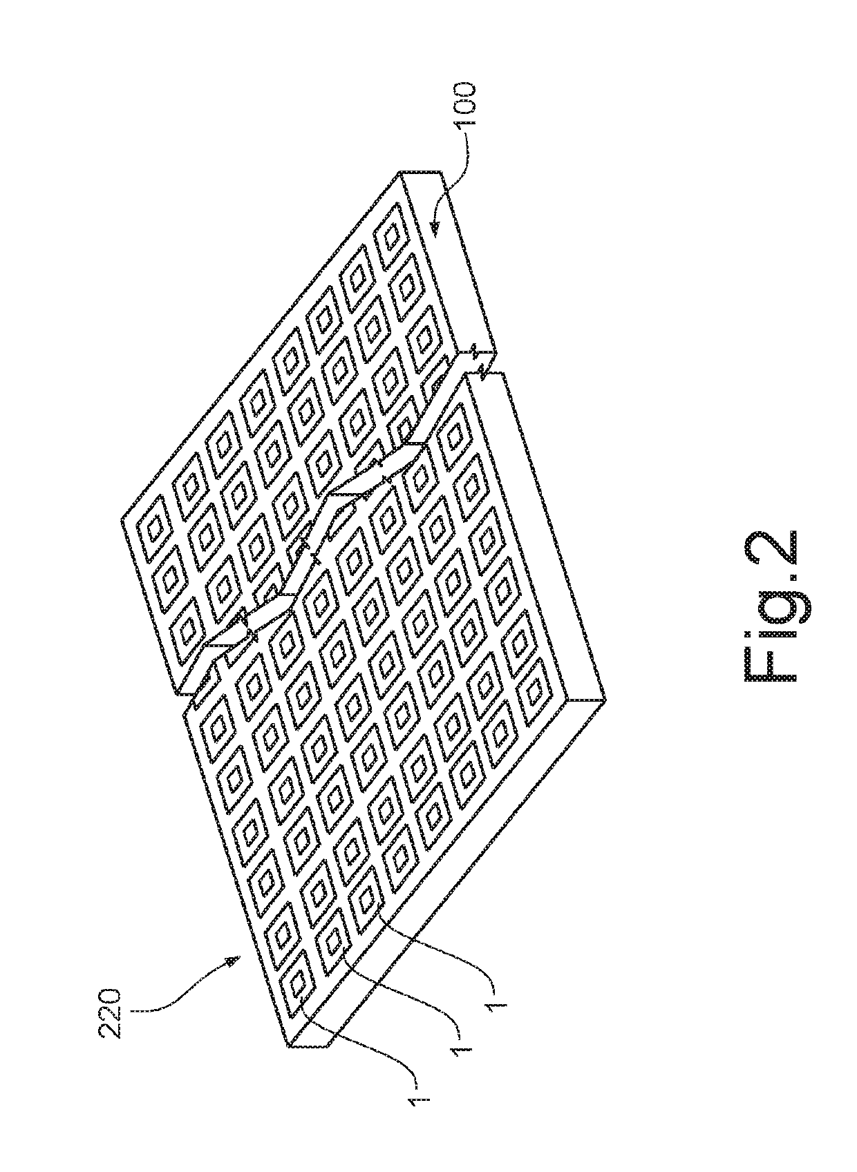
[0018]In greater detail, FIG. 1 shows a photodetector 1, which is integrated in a die 100 of semiconductor material. As illustrated in FIG. 2, the photodetector 1 may form part of an array 220 of photodetectors that are the same as one another, all designated by 1.

[0019]In detail, the photodetector 1 comprises a semiconductor body 3, which is made, for example, of silicon and in turn comprises a substrate 2, and a first epitaxial layer 6 and a second epitaxial layer 8. In FIG. 1, and likewise in the subsequent figures, the thicknesses of the substrate 2 and of the first and second epitaxial layers 6, 8 are not in scale, as neither are the thicknesses of the other regions, described hereinafter.

[0020]The substrate 2 is of an N++ type, has a thickness of, for example, between 300 μm and 500 μm, and has a doping level of, for example, between 1·1019 cm−3 and 1·1020 cm−1.

[0021]The first epitaxial layer 6 is of an N+ type, has a thickness of, for example, between 4 μm and 8 μm and overli...


PUM


Abstract

A photodetector includes a Geiger mode avalanche photodiode, which includes a body of semiconductor material, which is delimited by a front surface. The avalanche photodiode further includes: a cathode region having a first type of conductivity, which forms the front surface; and an anode region having a second type of conductivity, which extends in the cathode region starting from the front surface. The photodetector further includes: a dielectric region, arranged on the front surface; a quenching resistor, which extends on the dielectric region, is electrically connected to the anode region, and is laterally spaced apart with respect to the anode region; and an optical-isolation region, which extends through the dielectric region and laterally delimits a portion of the dielectric region, the anode region extending underneath the portion of the dielectric region, the optical-isolation region being moreover interposed between the portion of the dielectric region and the quenching resistor.

Description

BACKGROUNDTechnical Field[0001]The present disclosure relates to a photodetector including a Geiger mode avalanche photodiode (GMAP) and an integrated resistor as well as to the related manufacturing method.Description of the Related Art[0002]As is known, today available are avalanche photodiodes operating in Geiger mode, also known as single-photon avalanche diodes (SPADs), in so far as they enable, at least in theory, detection of single photons.[0003]In detail, it is known that a SPAD comprises a junction of semiconductor material, which presents a breakdown voltage VB and is biased, in use, at a reverse-biasing voltage VA higher in modulus than the breakdown voltage VB. In this way, the junction presents a particularly extensive depleted region, present in which is a non-negligible electrical field. Hence, generation of a single electron-hole pair, caused by absorption within the depleted region of a photon incident on the SPAD, may be sufficient for triggering an ionization pro...

Claims


Application Information

Patent Timeline
IPC IPC(8): H01L31/14H01L27/144H01L31/024H01L31/0216H01L31/0352H01L31/107H01L31/18G01J1/44
CPCH01L31/145G01J1/44H01L31/024G01J2001/4466G01J2001/442H01L27/1446H01L31/1864H01L31/02164H01L31/035281H01L31/107H01L31/1075
Inventor MAZZILLO, MASSIMO CATALDOCINNERA MARTINO, VALERIA
Owner STMICROELECTRONICS SRL
Why Eureka
Try Eureka