Electrostatic discharge circuit
a technology of electrostatic discharge and circuit, applied in the field of circuits, can solve problems such as damage to the integrated circui
- Summary
- Abstract
- Description
- Claims
- Application Information
AI Technical Summary
Benefits of technology
Problems solved by technology
Method used
Image
Examples
first embodiment
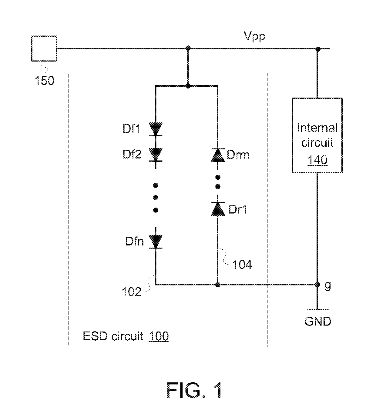
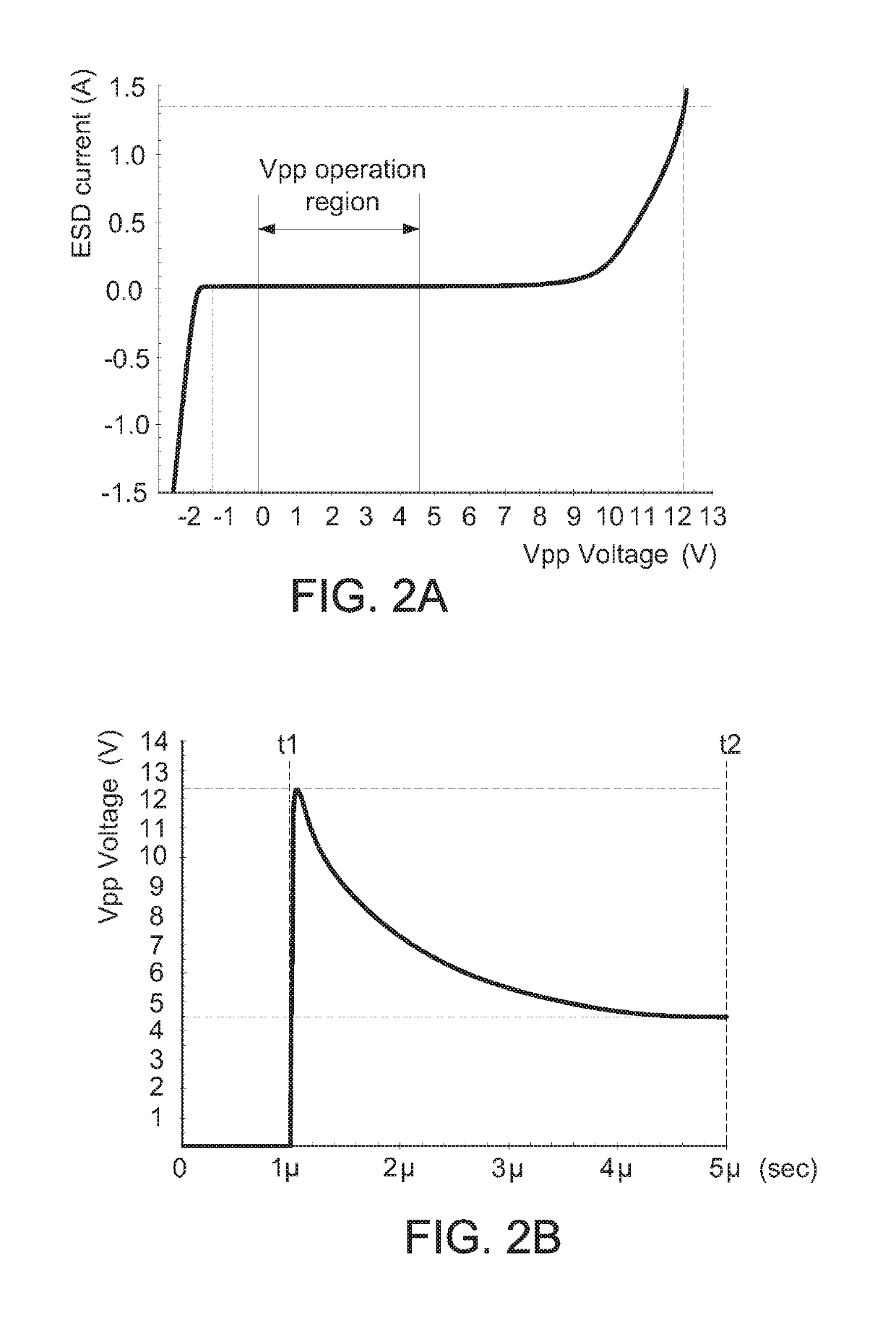
[0020]FIG. 1 is a schematic circuit diagram illustrating an ESD circuit according to the present invention. The ESD circuit 100 and an internal circuit 140 are connected between a power pad 150 of a first supply voltage Vpp and a node g of a second supply voltage GND. The first supply voltage Vpp is transmitted from the power pad 150 to the ESD circuit 100 and the internal circuit 140. The second supply voltage GND is transmitted to the ESD circuit 100 and the internal circuit 140 through the node g. In an embodiment, the second supply voltage GND is 0V.
[0021]The ESD circuit 100 comprises a first ESD current path 102 and a second ESD current path 104. The first ESD current path 102 comprises n diodes Df1˜Dfn. The n diodes Df1˜Dfn are connected between the power pad 150 and the node g in series. The second ESD current path 104 comprises m diodes Dr1˜Drm. The m diodes Dr1˜Drm are connected between the power pad 150 and the node g in series.
[0022]The turn-on threshold voltage of the fi...
second embodiment
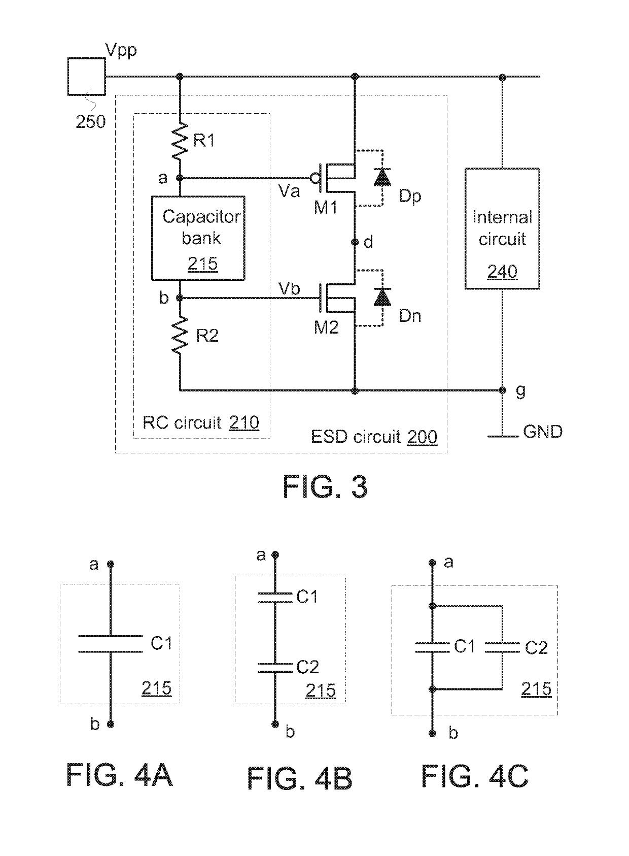
[0035]FIG. 3 is a schematic circuit diagram illustrating an ESD circuit according to the present invention. The ESD circuit 200 and an internal circuit 240 are connected between a power pad 250 of a first supply voltage Vpp and a node g of a second supply voltage GND. The first supply voltage Vpp is transmitted from the power pad 250 to the ESD circuit 200 and the internal circuit 240. The second supply voltage GND is transmitted to the ESD circuit 200 and the internal circuit 240 through the node g.
[0036]In this embodiment, the ESD circuit 200 comprises a RC circuit 210, a P-type transistor M1 and a N-type transistor M2. Moreover, the P-type transistor M1 maybe a P-type FinFET (Fin Field-effect transistor), and the N-type transistor M2 maybe a N-type FinFET. The P-type transistor M1 is connected between the power pad 250 and a node d. The N-type transistor M2 is connected between the node d and the node g. The RC circuit 210 is connected between the power pad 250 and the node g. Th...
third embodiment
[0056]FIG. 7 is a schematic circuit diagram illustrating an ESD circuit according to the present invention. In this embodiment, the ESD circuit 700 comprises a RC circuit 710, a P-type transistor M1 and a N-type transistor M2. The RC circuit 710 of the ESD circuit 700 is composed of transistors. Due to the connecting relationships between the transistors, some of the transistors have the resistive characteristics or the capacitive properties.
[0057]The RC circuit 710 comprises plural P-type transistors Mr1, Mr2, Mc1 and Mc2. Moreover, the P-type transistors Mr1, Mr2, Mc1 and Mc2 maybe P-type FinFETs. A first drain / source terminal and a body terminal of the P-type transistor Mr1 are connected to the power pad 250. A second drain / source terminal and a gate terminal of the P-type transistor Mr1 are connected to the node a. A first drain / source terminal and a body terminal of the P-type transistor Mr2 are connected to the node b. A second drain / source terminal and a gate terminal of the ...
PUM
 Abstract
Description
Claims
Application Information
 - R&D Engineer
- R&D Manager
- IP Professional
- Industry Leading Data Capabilities
- Powerful AI technology
- Patent DNA Extraction
Browse by: Latest US Patents, China's latest patents, Technical Efficacy Thesaurus, Application Domain, Technology Topic, Popular Technical Reports.
© 2024 PatSnap. All rights reserved.Legal|Privacy policy|Modern Slavery Act Transparency Statement|Sitemap|About US| Contact US: help@patsnap.com


