Method of forming a doped metal carbide film on a substrate and related semiconductor device structures

a metal carbide film and substrate technology, applied in semiconductor devices, chemical vapor deposition coatings, coatings, etc., can solve the problems of polysilicon not being ideal for advanced technology node applications, polysilicon not showing ideal effective work function (ewf) for both nmos and pmos devices, and the threshold voltage adjustment implantation process may become increasingly complex

Active Publication Date: 2019-11-14
ASM IP HLDG BV
View PDF0 Cites 229 Cited by
  • Summary
  • Abstract
  • Description
  • Claims
  • Application Information

AI Technical Summary

Problems solved by technology

However, doped polysilicon may not be an ideal gate electrode material for advanced technology node applications.
As a further example, polysilicon does not exhibit an ideal effective work function (eWF) for both NMOS and PMOS devices.
However, as device geometries reduce in advanced technology node applications, the th

Method used


Image

  • Method of forming a doped metal carbide film on a substrate and related semiconductor device structures
  • Method of forming a doped metal carbide film on a substrate and related semiconductor device structures
  • Method of forming a doped metal carbide film on a substrate and related semiconductor device structures

Examples


Embodiment Construction

[0017]Although certain embodiments and examples are disclosed below, it will be understood by those in the art that the invention extends beyond the specifically disclosed embodiments and / or uses of the invention and obvious modifications and equivalents thereof. Thus, it is intended that the scope of the invention disclosed should not be limited by the particular disclosed embodiments described below.

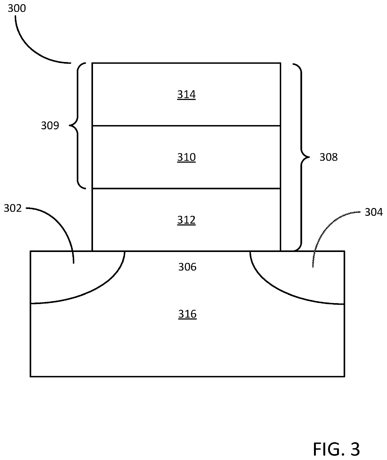
[0018]The illustrations presented herein are not meant to be actual views of any particular material, structure, or device, but are merely idealized representations that are used to describe embodiments of the disclosure.

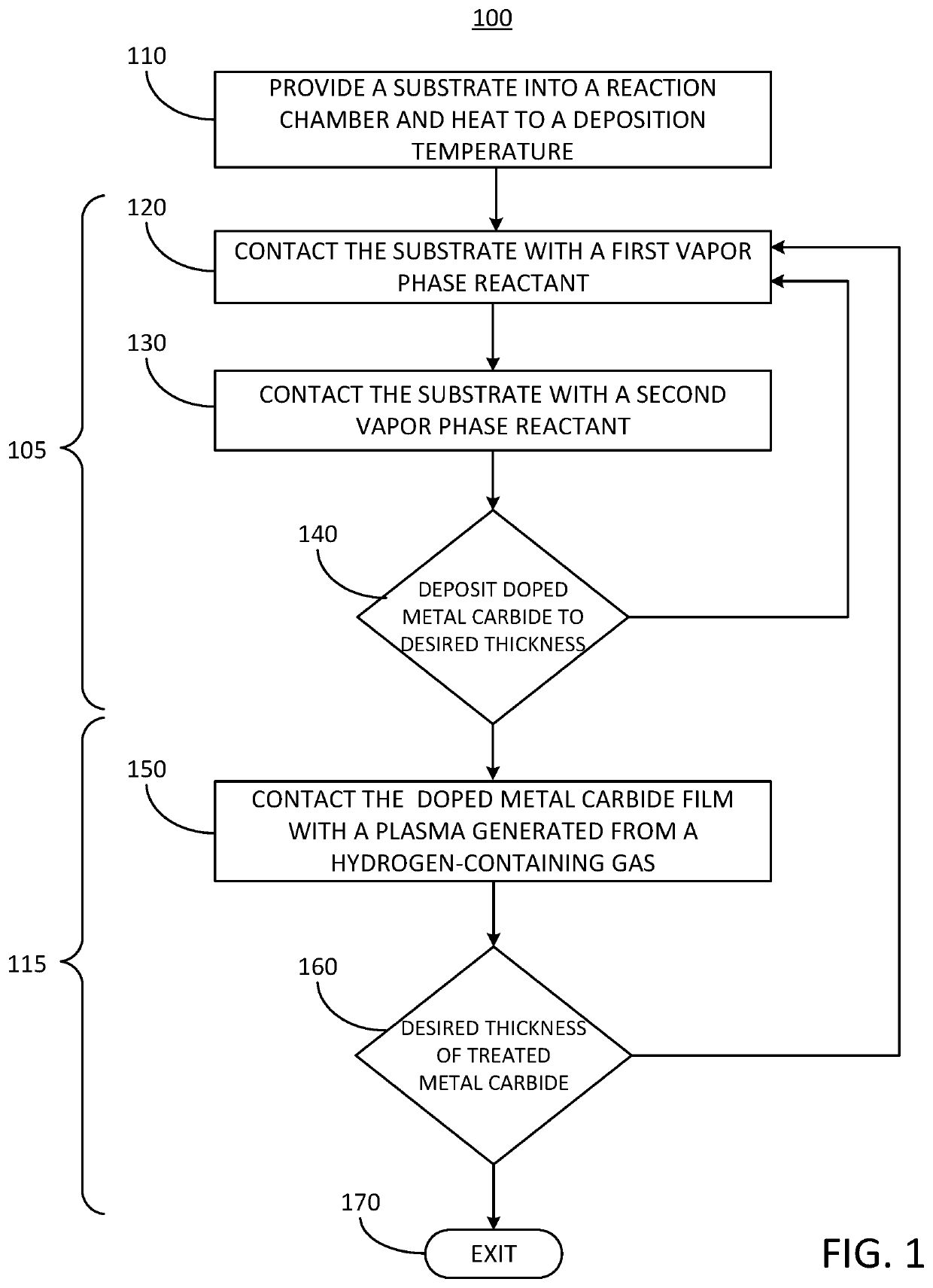
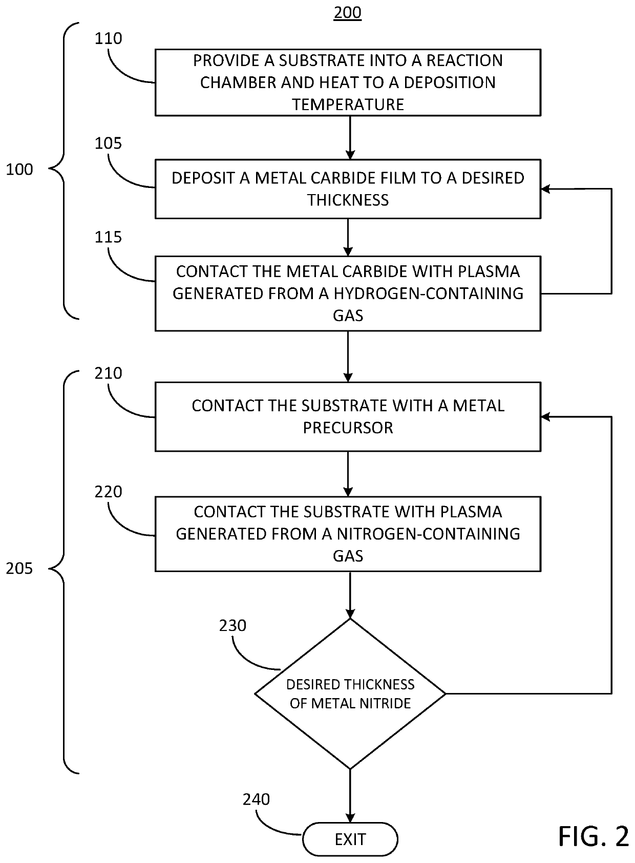
[0019]As used herein, the term “cyclical deposition” may refer to the sequential introduction of precursors (reactants) into a reaction chamber to deposit a film over a substrate and includes deposition techniques such as atomic layer deposition and cyclical chemical vapor deposition.

[0020]As used herein, the term “cyclical chemical vapor deposition” may refer to any p...


PUM

PropertyMeasurementUnit
Temperatureaaaaaaaaaa
Thicknessaaaaaaaaaa
Thicknessaaaaaaaaaa

Abstract

Methods for depositing a doped metal carbide film on a substrate are disclosed. The methods may include: depositing a doped metal carbide film on a substrate utilizing at least one deposition cycle of a cyclical deposition process; and contacting the doped metal carbide film with a plasma generated from a hydrogen-containing gas. Semiconductor device structures including a doped metal carbide film formed by the methods of the disclosure are also disclosed.

Description

CROSS-REFERENCE TO RELATED APPLICATIONS[0001]This application is a Non-Provisional of, claims priority to, and the benefit of, U.S. Ser. No. 62 / 670,312 filed May 11, 2018 and entitled “METHOD OF FORMING A DOPED METAL CARBIDE FILM ON A SUBSTRATE AND RELATED SEMICONDUCTOR DEVICE STRUCTURES,” which is hereby incorporated by reference in its entirety for all purposes.FIELD OF INVENTION[0002]The present disclosure relates generally to methods for forming a doped metal carbide film on a substrate and particularly to methods for depositing a doped metal carbide film on a substrate and subsequently contacting the doped metal carbide film with a plasma. The present disclosure is also related generally to semiconductor device structures comprising a doped metal carbide film deposited by a cyclical deposition process and a plasma treatment process.BACKGROUND OF THE DISCLOSURE[0003]Complementary metal-oxide-semiconductor (CMOS) technology has conventionally utilized n-type and p-type polysilico...

Claims


Application Information

Patent Timeline
IPC IPC(8): H01L29/423H01L29/49H01L21/28
CPCH01L29/4925H01L21/28088H01L29/42372C23C16/32C23C16/4554H01L29/4966H01L29/517H01L29/78H01L21/02041H01L21/02172H01L21/02205H01L21/02274H01L21/0228H01L21/02315H01L21/28556H01L21/324H01L21/8238
Inventor LI, DONGHSU, PENG-FURAISANEN, PETRIMOUSA, MOATAZ BELLAHJOHNSON, WARDCHEN, XICHONG
Owner ASM IP HLDG BV
Why Eureka
Try Eureka