Photoelectric detection structure and preparation method thereof

a detection structure and photoelectric technology, applied in the field of medical imaging diagnosis, can solve the problems of visible light divergence still present, increased incidence depth of rays, blurred image, etc., and achieves the effects of reducing light divergence, improving image definition, and improving light responsivity (conversion efficiency)

Inactive Publication Date: 2019-11-28
SHANGHAI IRAY TECH
View PDF3 Cites 6 Cited by
  • Summary
  • Abstract
  • Description
  • Claims
  • Application Information

AI Technical Summary

Benefits of technology

[0023]As described above, the photoelectric detection structure and the preparation method thereof provided by the present invention have the following beneficial effects:
[0024]The photoelectric detection structure and the preparation method thereof provided by the present invention can realize better image definition (decrease light divergence) and simultaneously can realize higher light responsivity (conversion efficiency).

Problems solved by technology

This structure has the problem that the absorption of most X rays in substances occurs near an incidence surface, but the produced visible light is in any direction.
A visible light emitting point is far from the visible light sensor below, the long transmission distance causes divergence of the visible light, which will consequently result in crosstalk of adjacent pixels and image blurred.
However, this solution still has another problem that, when high-energy rays with stronger permeability irradiate, the incidence depth of the rays is increased; and when the energy of the rays reaches a certain extent, the incidence depth can reach a position far away from the surface of the TFT sensor and the problem of divergence of visible light still exists.
Therefore, how to effectively solve the divergence of visible light in the flat-panel image sensor, decrease the crosstalk and improve the light responsivity has become one of problems which need to be urgently solved by one skilled in the art.

Method used


Image

  • Photoelectric detection structure and preparation method thereof
  • Photoelectric detection structure and preparation method thereof

Examples


embodiment 1

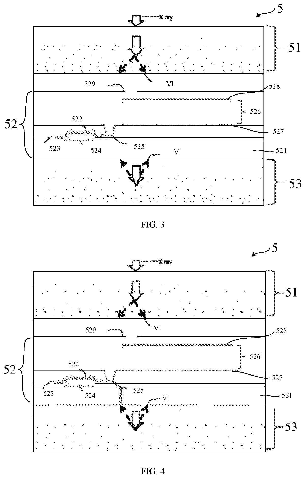
[0045]As illustrated in FIG. 3, the present invention provides a photoelectric detection structure 5, and the photoelectric detection structure 5 at least comprises:

[0046]a first scintillator layer 51, a first visible light sensor 52 and a second scintillator layer 53.

[0047]As illustrated in FIG. 3, the first scintillator layer 51 is located on an X ray receiving plane of the photoelectric detection structure 5 and is used for absorbing low-energy X rays and converting the X rays into visible light V1, and the visible light V1 becomes emergent from the first scintillator layer 51 and is detected by the first visible light sensor 52.

[0048]Specifically, a material of the first scintillator layer 51 includes but not limited to cesium iodide or gadolinium oxysulfide, any material which can convert X rays into visible light is applicable to the present invention and the material is not limited to this embodiment.

[0049]As illustrated in FIG. 3, the second scintillator layer 53 is located ...

embodiment 2

[0057]This embodiment provides a photoelectric detection structure, which is substantially the same as the structure in embodiment 1, the difference lies in that the substrate 521 is a fiber optical plate.

[0058]Specifically, as illustrated in FIG. 4, a plurality of fiber optical catheters perpendicular to a surface are provided in the fiber optical plate, the visible light produced by the second scintillator layer 53 is refracted to the first visible light sensor 52 through the fiber optical catheters and is absorbed, and thus the divergence of visible light can be effectively decreased.

embodiment 3

[0059]This embodiment provides a photoelectric detection structure, which is substantially the same as the structures in embodiment 1 and embodiment 2, the difference lies in that the lower layer of the second scintillator layer 53 further comprises a second visible light sensor (not shown) used for converting visible light penetrating through the second scintillator layer 53 into charges and storing the charges into the second visible light sensor.

[0060]Further, an extension may also be made to obtain an alternative distribution structure of a plurality of scintillator layers and a plurality of visible light sensors. The more the number of layers is, the shorter the passage of visible light is, the smaller the divergence of light is, the clearer the image is. Moreover, independent visible light sensors are used for different scintillator layers, the energy of X rays is higher, the irradiation depth is greater and thus multi-energy-level X ray detection can be achieved.


PUM


Abstract

A photoelectric detection structure and a preparation method, the structure comprises a first scintillator layer used for absorbing low-energy X rays and converting the X rays into visible light; a second scintillator layer used for absorbing high-energy X rays and converting the X rays into visible light; and a first visible light sensor located between the first scintillator layer and the second scintillator layer and used for converting visible light penetrating through the first scintillator layer and visible light reflected by the second scintillator layer into charges and storing the charges into the first visible light sensor. The method comprises providing a substrate, preparing layers layer by layer on the substrate through a semiconductor manufacturing process to form a first visible light sensor, forming a first scintillator layer on a first surface of the first visible light sensor and then forming a second scintillator layer on a second surface of the first visible light sensor.

Description

BACKGROUND OF THE PRESENT INVENTIONField of Invention[0001]The present invention relates to the field of medical imaging diagnosis, in particular to a photoelectric detection structure and a preparation method thereofDescription of Related Arts[0002]Flat-panel image sensors are usually applied to fields such as of medical radiation imaging, industrial flaw detection and security inspection. Flat-panel image sensors, especially large-size image sensors, usually have a size of several tens of centimeters and several millions to ten millions of pixels. In application of X-ray image detectors, it is generally required that the area reaches 43 cm*43 cm. Therefore, at present, the amorphous silicon technology is always adopted (monocrystalline silicon detectors generally have diameter of 24-30 cm at present).[0003]As illustrated in FIG. 1, a currently used amorphous silicon flat-panel detector is usually a multilayer stack structure and comprises upper-layer scintillators for converting i...

Claims


Application Information

Patent Timeline
Patent Type & Authority Applications(United States)
IPC IPC(8): G01T1/20
CPCG01T1/2008G01T1/2002G01T1/2018G01T1/20183G01T1/20186G01T1/20185
Inventor JIN, LIBO
Owner SHANGHAI IRAY TECH
Why Eureka
Try Eureka