Internal via with improved contact for upper semi-conductor layer of a 3D circuit

a 3d circuit and semi-conductor layer technology, applied in the field of integrated circuits, can solve problems such as space and integration difficulties, and achieve the effect of short duration

Active Publication Date: 2019-12-05
COMMISSARIAT A LENERGIE ATOMIQUE ET AUX ENERGIES ALTERNATIVES
View PDF4 Cites 4 Cited by
  • Summary
  • Abstract
  • Description
  • Claims
  • Application Information

AI Technical Summary

Benefits of technology

[0034]The thermal annealing carried out in the step d) can be advantageously a high-temperature annealing and of very short duration, typically carried out using a laser, and in particular a nanosecond laser with pulses that can have a duration of about ten nanoseconds.

Problems solved by technology

Such an arrangement of a connection structure can give rise to problems concerning space.
Such a connection structure gives rise to integration difficulties and comprises high access resistance with the active zone of the transistor.
There is the problem of carrying out a new improved connection structure with regards to one or the other of the disadvantages mentioned hereinabove.

Method used


Image

  • Internal via with improved contact for upper semi-conductor layer of a 3D circuit
  • Internal via with improved contact for upper semi-conductor layer of a 3D circuit
  • Internal via with improved contact for upper semi-conductor layer of a 3D circuit

Examples


Embodiment Construction

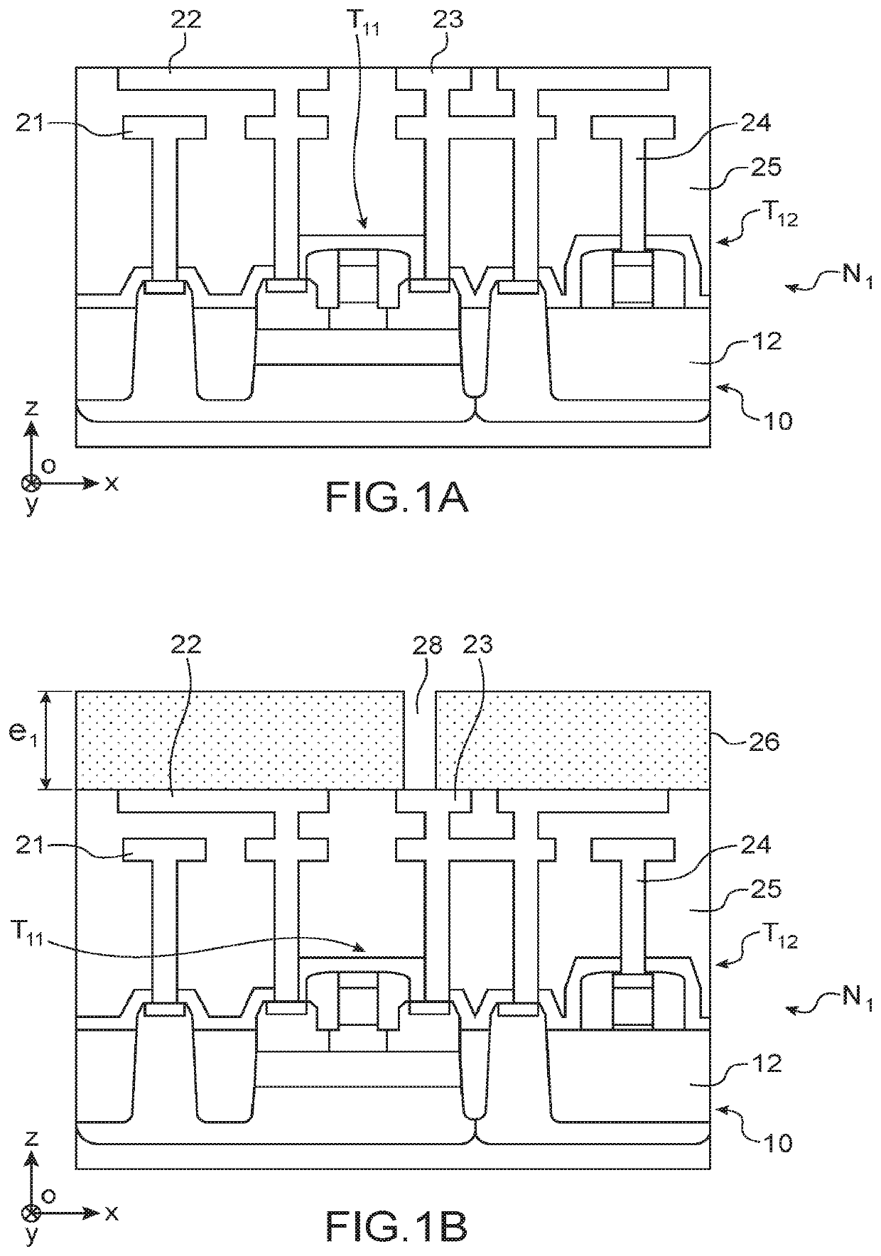
[0050]Reference is now made to FIG. 1A that gives a possible starting device for implementing a method for producing a connection structure in a 3D circuit comprising several semi-conductor layers arranged one above the other.

[0051]The connection structure that is produced here comprises a contact zone with a metal and semi-conductor compound, in particular a silicide contact zone, formed in this example under an active zone of a higher level transistor, in other words under a semi-conductor layer wherein this higher level transistor is at least partially carried out.

[0052]The starting device can be carried out using a substrate that comprises a first superficial semi-conductor layer 12 wherein one or several electronic components of a first level N1 of electronic components are provided. In the example shown in FIG. 1A, the electronic components are transistors T11 and T12, and have respective channel regions that extend in the first semi-conductor layer 12. The transistors T11, T1...


PUM


Abstract

Connection structure for microelectronic device with superposed semi-conductor layers comprising a conductor via that connects a lower face of an upper semi-conductor layer and an underlying conducting zone, said connection structure further comprising a silicide zone in contact with a lower face or with an inner face of the layer of the upper semi-conductor layer.

Description

TECHNICAL FIELD AND PRIOR ART[0001]This application relates to the field of integrated circuits provided with components distributed over several levels or stages of electronic components.[0002]Such devices are generally qualified as three-dimensional or “3D” integrated circuits and typically comprise at least one first semi-conductor layer referred to as “lower” and at least one second semi-conductor layer referred to as “upper”, with the second semi-conductor layer being arranged above the first semi-conductor layer and separated from the first semi-conductor layer by at least one insulating layer.[0003]In a device with transistors T1, T2 distributed over several levels, in order to establish a connection between a transistor T2 of an upper level and a conducting zone located under this upper level, typically in the form of a metal line 8, a connection structure such as in FIG. 9 can be provided.[0004]This connection structure is formed from a vertical pad 5 in contact with the ac...

Claims


Application Information

Patent Timeline
Patent Type & Authority Applications(United States)
IPC IPC(8): H01L21/822H01L21/768H01L23/535H01L27/06
CPCH01L21/8221H01L27/0688H01L23/535H01L21/76895H01L21/76889H01L21/76805H01L21/28518H01L21/76898H01L21/823475
Inventor FENOUILLET-BERANGER, CLAIRENEMOUCHI, FABRICEVINET, MAUD
Owner COMMISSARIAT A LENERGIE ATOMIQUE ET AUX ENERGIES ALTERNATIVES
Why Eureka
Try Eureka