
Display device and method for manufacturing the same

Inactive Publication Date: 2019-12-19
INT TECH HK CO LTD
View PDF0 Cites 0 Cited by
  • Summary
  • Abstract
  • Description
  • Claims
  • Application Information

AI Technical Summary

Benefits of technology

The patent provides a method for making a display device by applying a special gel-like material onto the surface of a thin-film layer made of aluminum. The gel-like material is then cured using UV radiation to form a cover layer. This process does not harm the organic light-emitting element, which is sensitive to heat. The technical effect of this method is that it helps to improve the durability and reliability of the display device.

Problems solved by technology

Moreover, consumers demand thin display devices.

Method used


Image

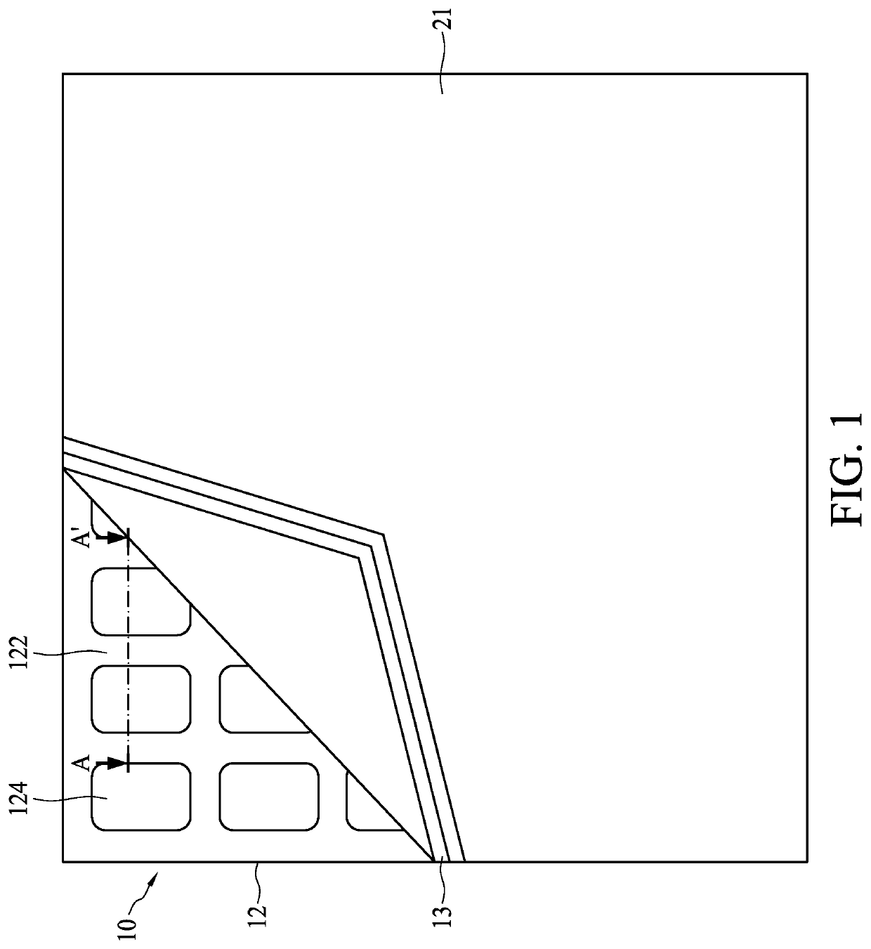
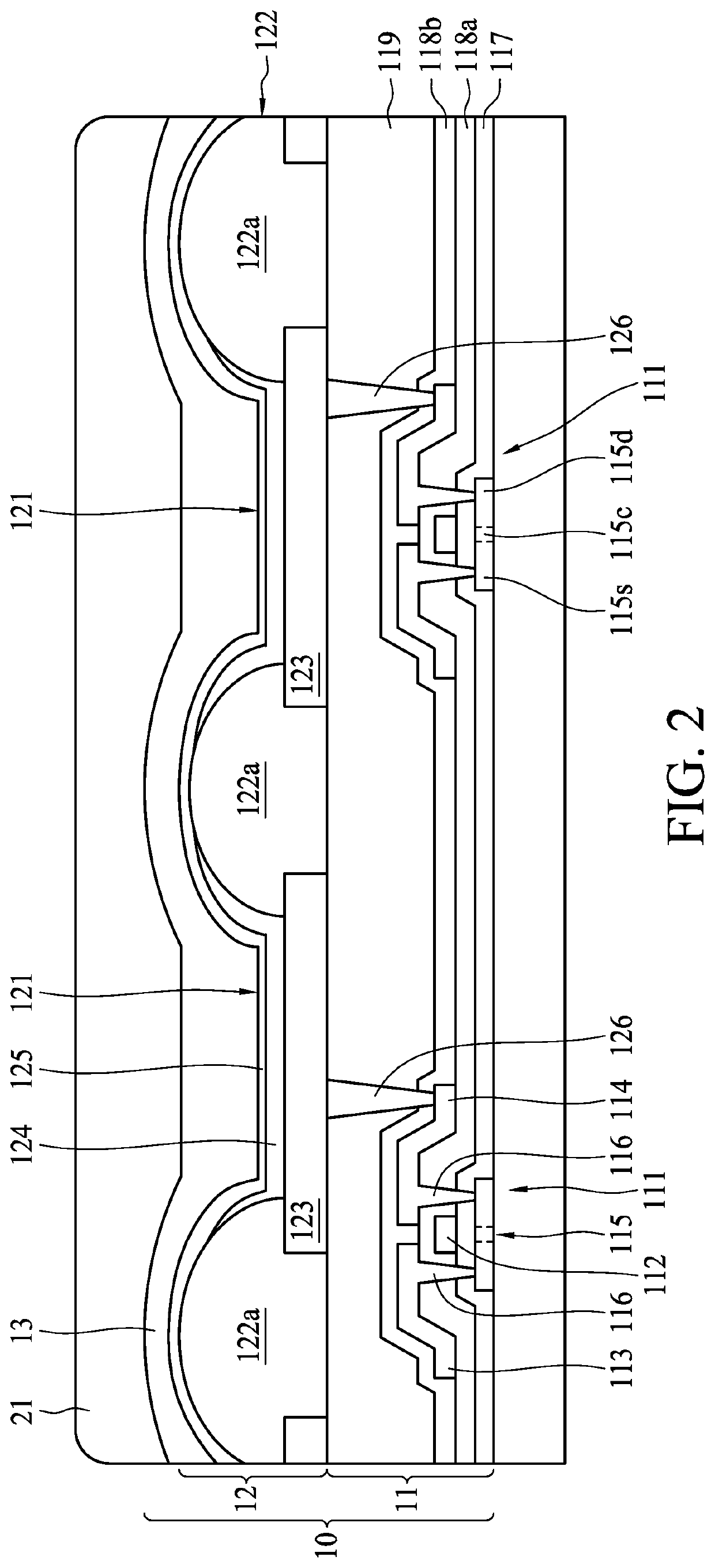
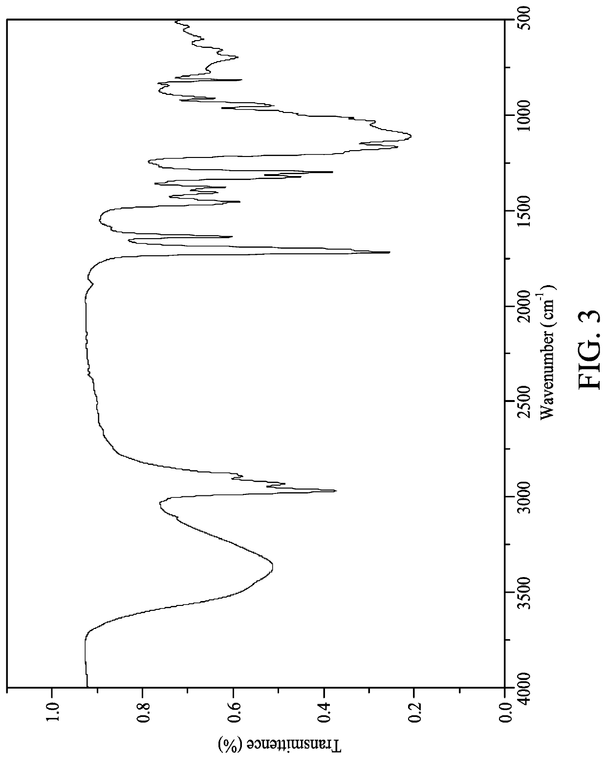
  • Display device and method for manufacturing the same
  • Display device and method for manufacturing the same
  • Display device and method for manufacturing the same

Examples


embodiment 1

[0060]44 wt % (relative weight, same as below) of 3-methylacryloxypropyl trimethoxysilane, 0.22 wt % of oxalic acid, 9.53 wt % of deionized water and 46.11 wt % of 2-butanol were fully stirred under room temperature and normal pressure so that the reactants were mixed uniformly and subjected to polymerization reaction, thereby obtaining a silicon sol-gel (hereinafter, 44%-silicon sol-gel).

embodiment 2

[0061]30.56 wt % (relative weight, same as below) of 3-methylacryloxypropyl trimethoxysilane, 0.30 wt % of oxalic acid, 14.42 wt % of deionized water and 54.7 wt % of 2-butanol were fully stirred under room temperature and normal pressure so that the reactants were mixed uniformly and subjected to polymerization reaction, thereby obtaining a silicon sol-gel (hereinafter, 30%-silicon sol-gel).

embodiment 3

[0062]First, 41.8 wt % of sec-butanol aluminum [Al(OC4H9), abbreviated as ASB below] and 35.0 wt % of 2-butanol were mixed uniformly at 85 to 90° C. Then, 22.05 wt % of ethyl acetoacetate (EAcAc) was added as the chelating agent for ASB, and 1.13 wt % of nitric acid was added as the catalyst, the reactants were refluxed for 7-8 hours for polymerization reaction, thereafter, the mixture was cooled and filtered with a 0.22 μm filter, thereby obtaining an aluminum sol-gel.


PUM

PropertyMeasurementUnit
Temperatureaaaaaaaaaa
Transmittivityaaaaaaaaaa
Temperatureaaaaaaaaaa

Abstract

A display device includes an organic light emitting element and a cover layer. The organic light emitting element includes a thin-film encapsulation layer comprising an aluminum-containing material. The cover layer is disposed on the thin-film encapsulation layer, and the cover layer includes a silicon containing unit, an aluminum containing unit, and a bridging unit, and the aluminum-containing unit of the covering layer is covalently bonded to the thin-film encapsulating layer. A method of manufacturing a display device includes providing a dual-curable sol-gel composition comprising a silicon-containing monomer, an aluminum-containing monomer, a solvent, and a polymerization initiator, applying the composition to a thin-film encapsulation layer of an organic light-emitting device; and curing the composition with a UV radiation and at a curing temperature to form a cover layer on the thin-film encapsulation layer, wherein the curing temperature is a temperature that does not damage the organic light-emitting element.

Description

PRIORITY CLAIM AND CROSS REFERENCE[0001]This application claims priority to U.S. patent provisional application No. 62 / 684,778, filed on Jun. 14, 2018, which is incorporated by reference in its entirety.FIELD OF INVENTION[0002]The present disclosure relates generally to a display device and a method for manufacturing the same; particularly to a display device with a cover layer and a method for manufacturing the same.BACKGROUND[0003]Display devices (such as display devices comprising organic light-emitting diodes (OLED)) have been integrated in various electronic devices, such as smartphones, for displaying.[0004]As electronic devices evolve into various forms, display devices change accordingly; for example, display devices have to be flexible, durable, etc. Moreover, consumers demand thin display devices. In addition to integrated various functional components into the display device, more attention should be paid to the thickness of the display device.BRIEF SUMMARY OF THE INVENTI...

Claims


Application Information

Patent Timeline
IPC IPC(8): H01L51/52C09D183/08C09D163/00C09D133/08
CPCH01L2251/30C09D183/08C09D163/00H01L51/5253C09D133/08C09D1/00H10K59/873H10K71/40C09D4/00C09D183/14C08G77/58C08F230/085H10K50/844H10K2102/00
Inventor KU, CHUNKANGLU, YUCHILAN, YIHSIN
Owner INT TECH HK CO LTD
Features
  • Generate Ideas
  • Intellectual Property
  • Life Sciences
  • Materials
  • Tech Scout
  • Unparalleled Data Quality
  • Higher Quality Content
  • 60% Fewer Hallucinations
Learn More