

Magnetoresistance effect element
a technology of magnetic effect and element, applied in the field of magnetic effect element, can solve the problems of difficulty in enhancing output voltage value, and achieve the effects of less lattice mismatch, better bias dependency of voltage, and higher mr ratio
- Summary
- Abstract
- Description
- Claims
- Application Information
AI Technical Summary
Benefits of technology
Problems solved by technology
Method used
Image

Examples
first embodiment
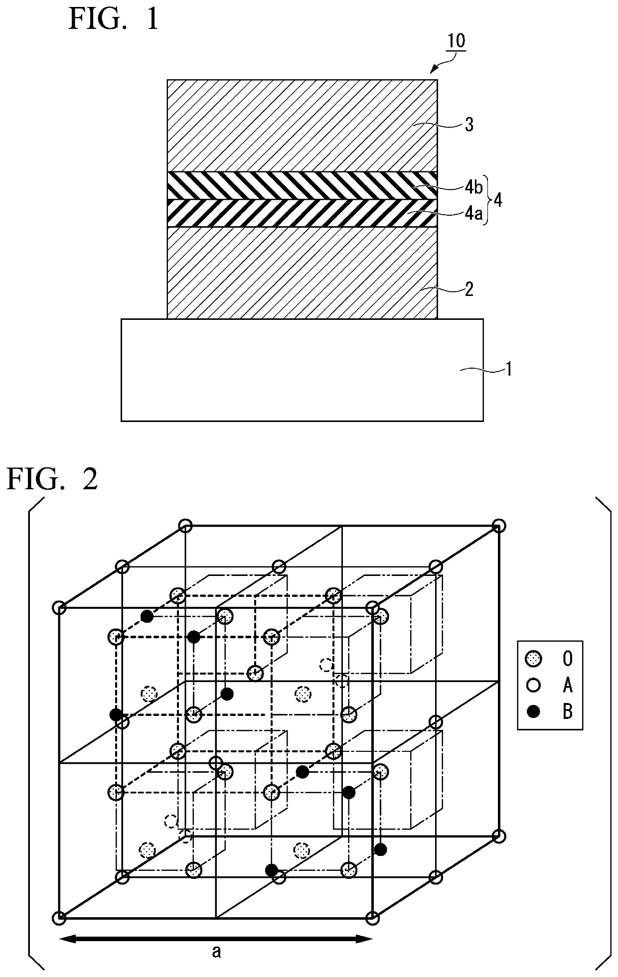
[0033]FIG. 1 is a sectional view schematically illustrating a magnetoresistance effect element according to a first embodiment of the disclosure. The magnetoresistance effect element 10 illustrated in FIG. 1 includes a substrate 1, a first ferromagnetic layer 2, a second ferromagnetic layer 3, and a tunnel barrier layer 4. The magnetoresistance effect element 10 may include a cap layer and a buffer layer in addition to the above-mentioned layers.
[0034]Substrate It is preferable that the substrate 1 have excellent flatness. For example, MgO, Si, or AlTiC can be used as the material of the substrate 1.
[0035]First ferromagnetic layer and second ferromagnetic layer The first ferromagnetic layer 2 and the second ferromagnetic layer 3 have magnetization. The magnetoresistance effect element 10 outputs a change in relative angle of the magnetization as a change in resistance value. For example, when a magnetization direction of the second ferromagnetic layer 3 is fixed and a magnetization ...
second embodiment
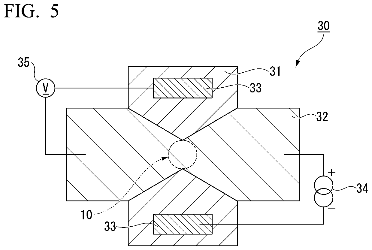
[0069]FIG. 4 is a sectional view schematically illustrating a magnetoresistance effect element according to a second embodiment of the disclosure. In the magnetoresistance effect element 20 according to the second embodiment, the same elements as in the magnetoresistance effect element 10 according to the first embodiment will be referred to by the same reference signs and description thereof will not be repeated.
[0070]In the magnetoresistance effect element 20 illustrated in FIG. 4, a tunnel barrier layer 24 is a stacked body which includes two first oxide layers 4a and in which a second oxide layer 4b is interposed between the two first oxide layers 4a. The first oxide layer 4a contains element A and element B at an atomic ratio (element A:element B) of 1−x:x (04b contains element A and element B at an atomic ratio (element A:element B) of 1−y:y (04a are oxide layers containing more element A in comparison with the second oxide layer 4b and thus have higher crystallinity. The comp...
PUM
| Property | Measurement | Unit |
|---|---|---|
| thickness | aaaaa | aaaaa |
| magnetoresistance | aaaaa | aaaaa |
| thickness | aaaaa | aaaaa |
Abstract
Description
Claims
Application Information