
Low Noise Quantized Feedback Configuration

a quantized feedback and low noise technology, applied in the field of sigmadelta modulators, can solve the problems of adding complexity and cost, and achieve the effect of improving the performance of modulators

Active Publication Date: 2020-01-02
SILICONINTERVENTION INC
View PDF0 Cites 1 Cited by
  • Summary
  • Abstract
  • Description
  • Claims
  • Application Information

AI Technical Summary

Benefits of technology

The patent describes a way to make ΣΔ modulators work better.

Problems solved by technology

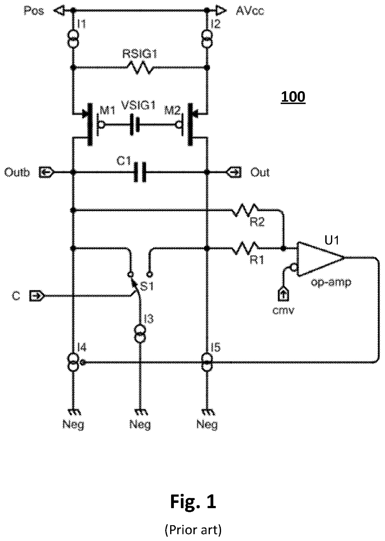
The common mode control portion of the circuit 100, i.e., the components below transistors M1 and M2, adds complexity and cost.

Method used


Image

  • Low Noise Quantized Feedback Configuration
  • Low Noise Quantized Feedback Configuration
  • Low Noise Quantized Feedback Configuration

Examples


Embodiment Construction

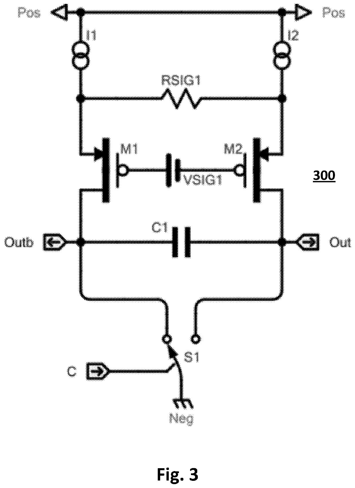
[0017]The present application describes an improved ΣΔ modulator, which may function as an ADC. In one embodiment, the ΣΔ modulator has no common mode control loop, and no reference current. This results in decreased complexity, i.e., fewer components, as well as reduced noise.

[0018]As explained above, FIG. 1 shows an example of a ΣΔ modulator circuit 100 of the prior art, in which an input difference current is made to flow in the drains of transistors M1 and M2. This occurs because a portion of the nominally equal currents of the current sources I1 and I2 flows through the resistor RSIG1 due to the input voltage VSIG1, which is applied to the gates of transistors M1 and M2.

[0019]This configuration of the upper portion of circuit 100, with current sources I1 and I2, transistors M1 and M2, resistor RSIG1 and an input voltage source VSIG1, is well known to those of skill in the art, and makes what is commonly called a voltage-to-current (V to I) convertor. The V to I convertor conver...


PUM


Abstract

Described herein is an improved apparatus for increasing the performance of a ΣΔ modulator, which may function as an ADC. In one embodiment, the ΣΔ modulator comprises a voltage to current converter, a capacitor connected between two outputs of the voltage to current converter to receive a differential input current, and a switch that can switch between connecting each output of the voltage to current converter to ground while disconnecting the other output of the voltage to current converter. In this embodiment, the ΣΔ modulator has no common mode control loop, and no reference current. This results in decreased complexity, i.e., fewer components, as well as reduced noise.

Description

[0001]This application claims priority from Provisional Application No. 62 / 691,504, filed Jun. 28, 2018, which is incorporated by reference herein in its entirety.FIELD OF THE INVENTION[0002]The present invention relates generally to sigma-delta modulators, and more particularly to sigma-delta modulators without common mode control loops.BACKGROUND OF THE INVENTION[0003]Quantized feedback may be used in control loops to perform analog to digital conversion. Analog to digital converters (ADCs) with such features are often known as sigma-delta (ΣΔ) converters, or ΣΔ modulators, the modulator term referring to an output digital data stream having a certain symbol pattern, or modulation, imposed upon it by the control loop. The terms ΣΔ modulator and noise shaping control loop are often used interchangeably in the art, although the latter is more descriptive. Circuit designers often like to use such ΣΔ modulators as in many cases they may be simpler to design and cheaper to make than ot...

Claims


Application Information

Patent Timeline
IPC IPC(8): H03M3/00
CPCH04B1/0017H04L25/061H03M3/30H03M1/1057H04B1/1027H03M3/39H03M3/43H03M3/456
Inventor MALLINSON, A. MARTIN
Owner SILICONINTERVENTION INC
Learn More