
Inspection system and malfunction analysis/prediction method for inspection system

a technology of inspection system and malfunction analysis, applied in the field of inspection system, can solve the problems of difficult to identify the location of malfunction and difficult to sufficiently predict malfunction, and achieve the effect of quick specification or estimation of malfunction location and improved operation rate of inspection system

Active Publication Date: 2020-01-09
TOKYO ELECTRON LTD
View PDF0 Cites 1 Cited by
  • Summary
  • Abstract
  • Description
  • Claims
  • Application Information

AI Technical Summary

Benefits of technology

The present invention helps to quickly identify the cause of malfunctions in a prober or tester by analyzing their history information. This allows for timely replacement or repair of malfunctioning components, which improves the operation rate of the inspection system.

Problems solved by technology

In this case, even if each of the tester and the prober has the diagnosis function, it is difficult to identify the location of the malfunction.
Further, it is also difficult to sufficiently predict the malfunction when the prober is diagnosed as FAIL (NG) due to the malfunction caused in the tester, or vice versa.

Method used


Image

  • Inspection system and malfunction analysis/prediction method for inspection system
  • Inspection system and malfunction analysis/prediction method for inspection system
  • Inspection system and malfunction analysis/prediction method for inspection system

Examples


Embodiment Construction

[0028]Hereinafter, embodiments will be described in detail with reference to the accompanying drawings.

[0029]

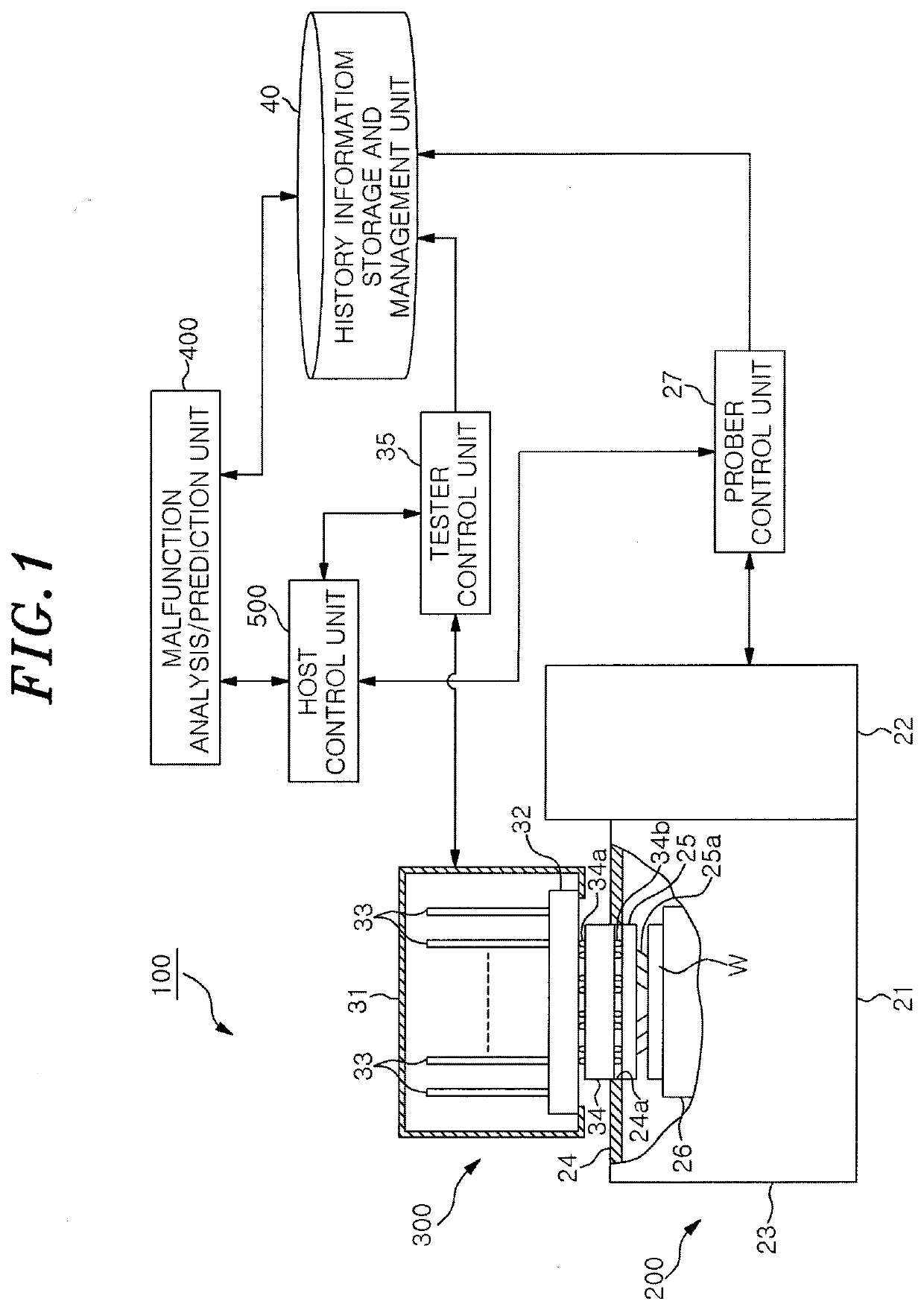
[0030]FIG. 1 schematically shows a configuration of an inspection system according to an embodiment of the present invention. The inspection system is configured to perform an electrical inspection of multiple devices (IC chips; hereinafter, also referred to as “Device Under Test (DUT)”) formed on a wafer after all necessary processes are performed on the wafer.

[0031]As shown in FIG. 1, an inspection system 100 includes a prober 200 for bringing probes of a probe card into contact with devices on a wafer, a tester 300 for applying electrical signals to the devices to perform an electrical inspection, a malfunction analysis / prediction unit 400, and a host control unit 500.

[0032]The prober 200 includes a main body 21, a transport unit 22, and a prober control unit 27.

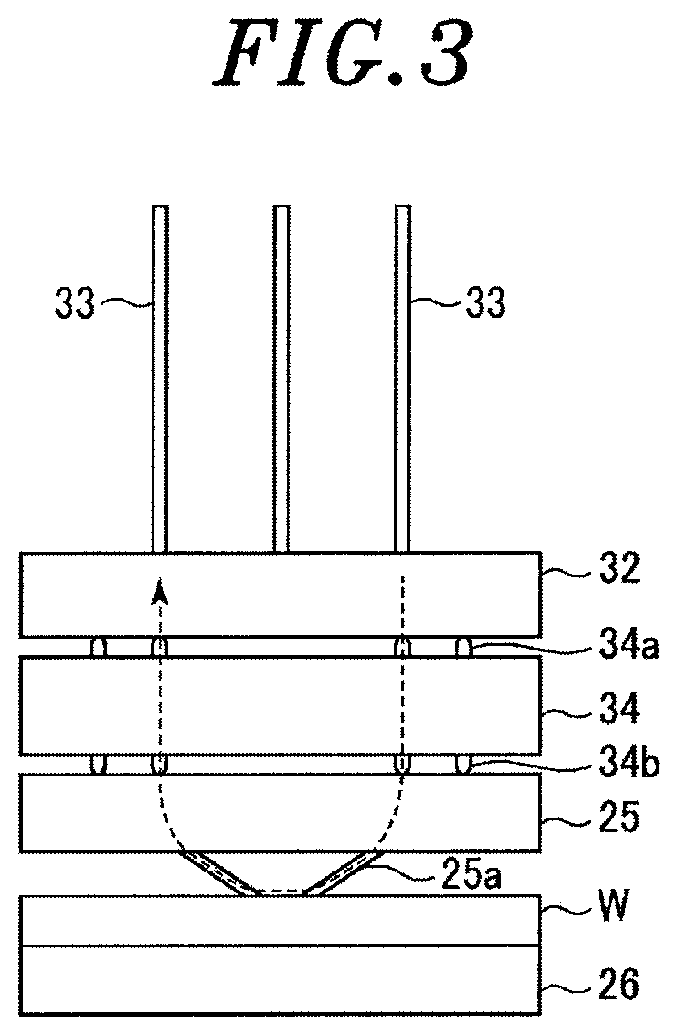
[0033]The main body 21 has a housing 23, a head plate 24 forming an upper surface of the housing 23 and having a...


PUM


Abstract

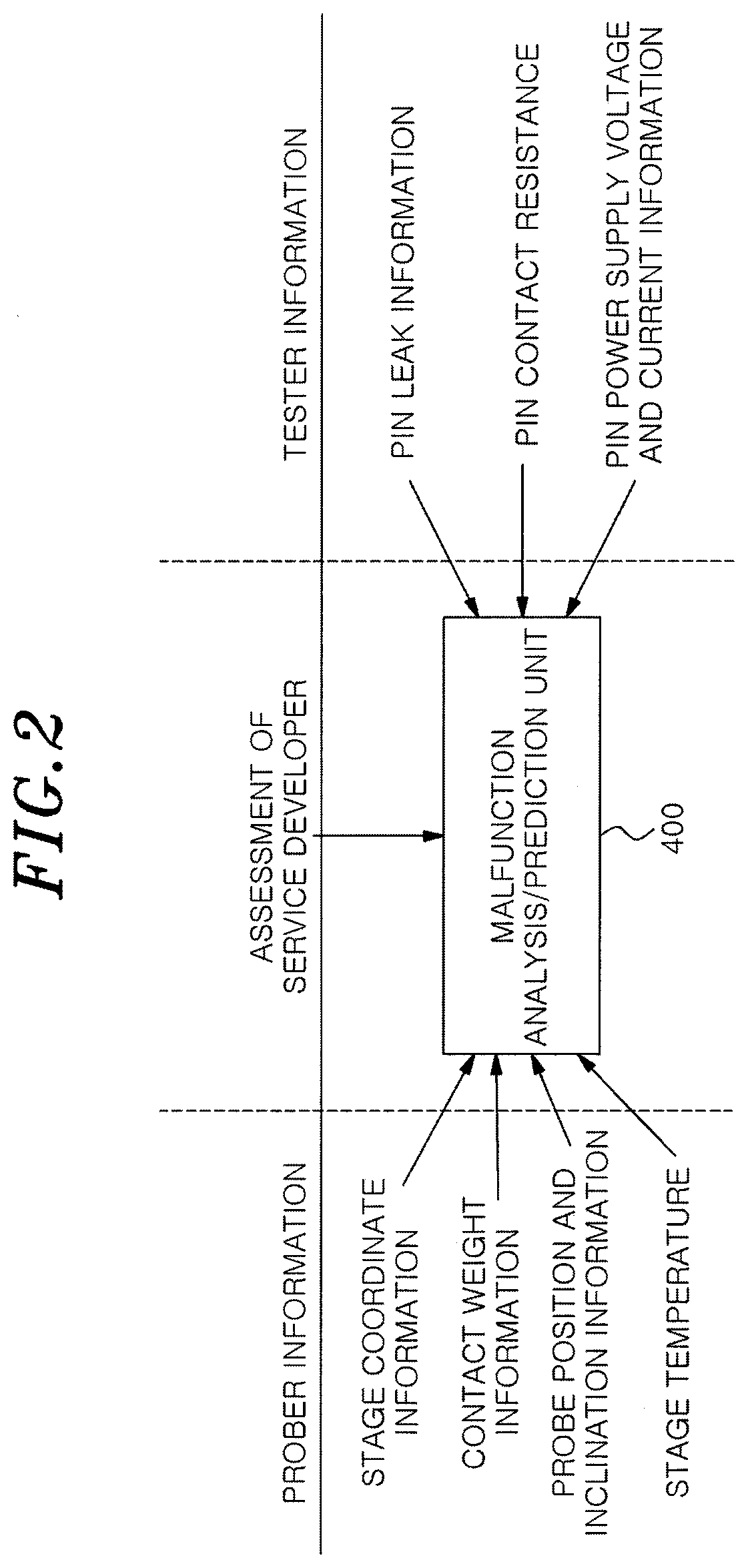
An inspection system includes a prober, a tester and a malfunction analysis / prediction unit. The prober has a stage holding a substrate having multiple devices formed thereon, a transport unit that transfers the substrate to the stage, and a probe card that brings a plurality of probes into contact with electrodes of the multiple devices on the substrate. A tester applies electrical signals to the multiple devices on the substrate through the probe card and inspects electrical characteristics of the multiple devices. The malfunction analysis / prediction unit, when a malfunction or a sign indicating a stage leading to the malfunction has occurred during an inspection, analyzes history information of the prober and tester related to the malfunction to determine or predict a location of the malfunction.

Description

TECHNICAL FIELD[0001]The present invention relates to an inspection system for inspecting a target object to be inspected and a malfunction analysis / prediction method for the inspection system.BACKGROUND[0002]In a semiconductor device manufacturing process, electrical inspection of multiple devices (IC chips) formed on a semiconductor wafer (hereinafter, simply referred to as “wafer”) is performed after all processes are performed on the wafer. An inspection system for performing such an electrical inspection generally includes a wafer stage, a wafer transfer system, a prober provided with a probe card having probes to be in contact with the devices formed on the wafer, and a tester for testing various electrical characteristics of the devices by applying electrical signals to the devices.[0003]In this inspection system, it is required to quickly identify a cause of a malfunction when the malfunction has occurred to quickly deal with the malfunction. Further, it is also required to ...

Claims


Application Information

Patent Timeline
Patent Type & Authority Applications(United States)
IPC IPC(8): G01R31/28G01R1/067G01R31/26H01L21/67H01L21/66
CPCG01R31/2831G01R31/26G01R1/067H01L21/67288H01L22/20G01R31/2891G01R35/00G01R31/31718G01R31/2851G01R1/07307G05B23/0283H01L21/67242H01L22/30H01L22/14
Inventor KAGAMI, TETSUYA
Owner TOKYO ELECTRON LTD
Learn More