Photonic crystal ink composition comprising light-absorbing nanoparticles and photonic crystal structure formed using the same
a technology of photonic crystals and inks, which is applied in the field of ink compositions, can solve the problems of poor color sharpness, lowering the value of use of materials as coating materials, and deteriorating the aesthetic properties of materials, and achieves the effect of suppressing white scattering and high color sharpness
- Summary
- Abstract
- Description
- Claims
- Application Information
AI Technical Summary
Benefits of technology
Problems solved by technology
Method used
Image
Examples
example 1
[0086](1) Preparation of Photonic Crystal Composition
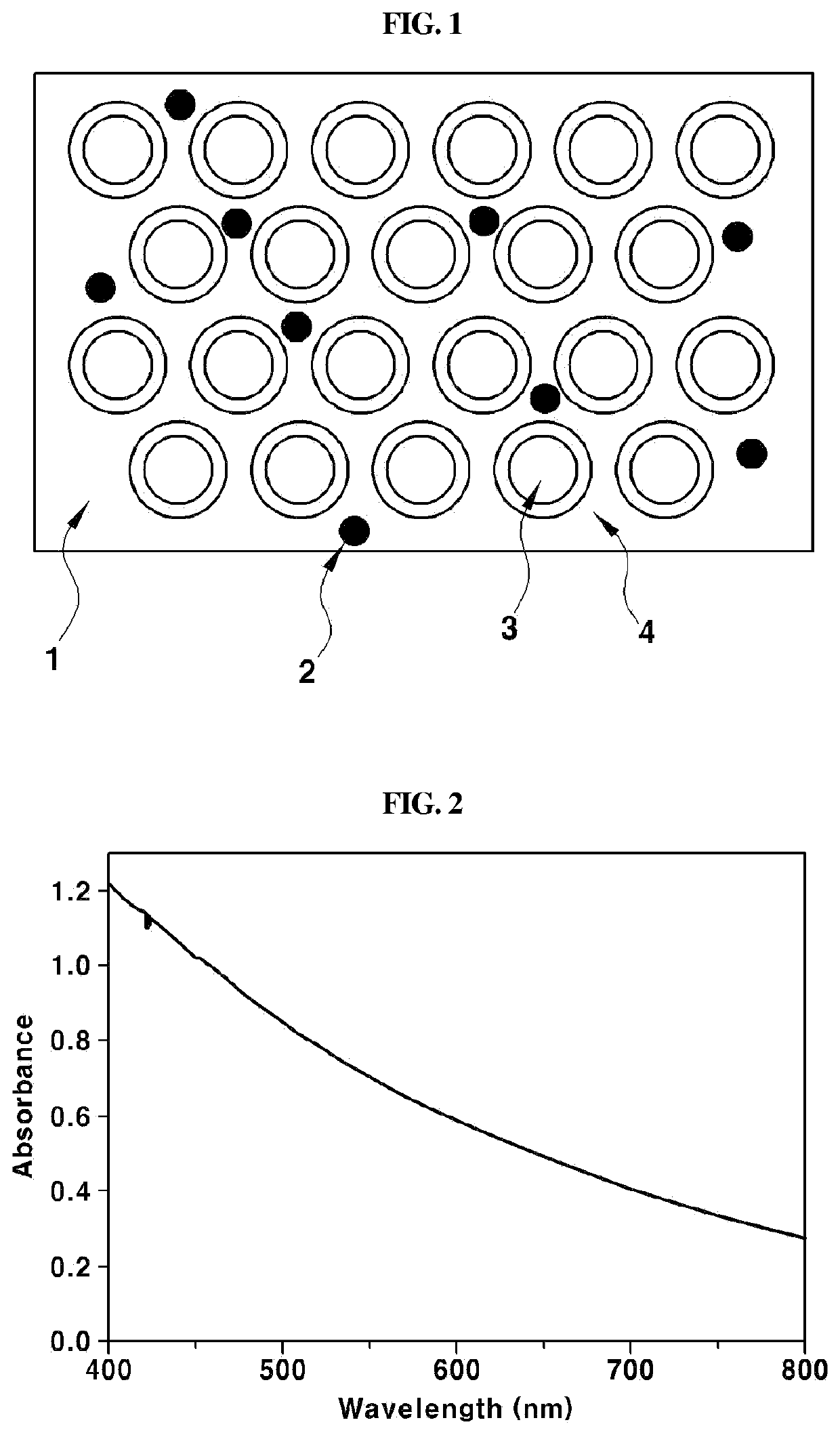
[0087]Silica particles were dispersed such that the volume ratio of silica particles and ethoxylated trimethylol propane triacrylate (ETPTA) containing a photoinitiator was 33% (v / v), and melanin nanoparticles were further added thereto and mixed, thus preparing a photonic crystal ink composition.
[0088]As such, the mixing process was performed using a vortex mixer, after which the extent of mixing was increased using a sonicator.
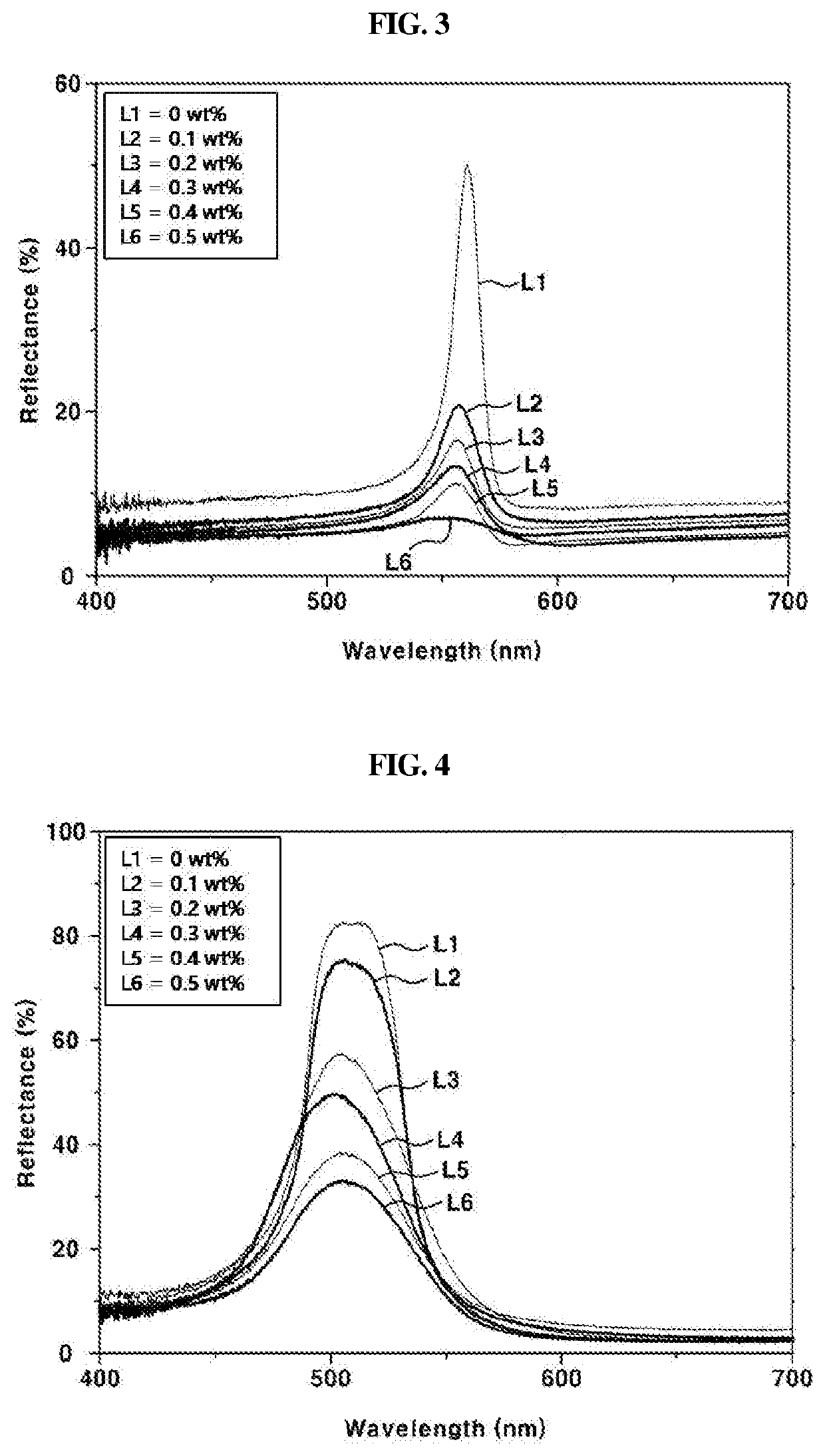
[0089]As the photoinitiator, hydroxyl cyclohexyl phenyl ketone was added in an amount of 0.1 wt % based on the amount of the photonic crystal ink composition, and melanin nanoparticles were added in an amount of 0.1 wt %.
[0090]Furthermore, the melanin nanoparticles had an average particle size of 100 nm and the silica particles had an average particle size of 173 nm.
[0091](2) Formation of Photonic Crystal Structure (Film)
[0092]The photonic crystal ink composition was made to penetrate between two glass pla...
examples 2 to 5
[0095]Respective photonic crystal structures and porous structures were manufactured in the same manner as in Example 1, with the exception that the amount of the melanin nanoparticles was adjusted to 0.2 wt % (Example 2), 0.3 wt % (Example 3), 0.4 wt % (Example 4), and 0.5 wt % (Example 5).
example 6
[0103](1) Preparation of Photonic Crystal Composition
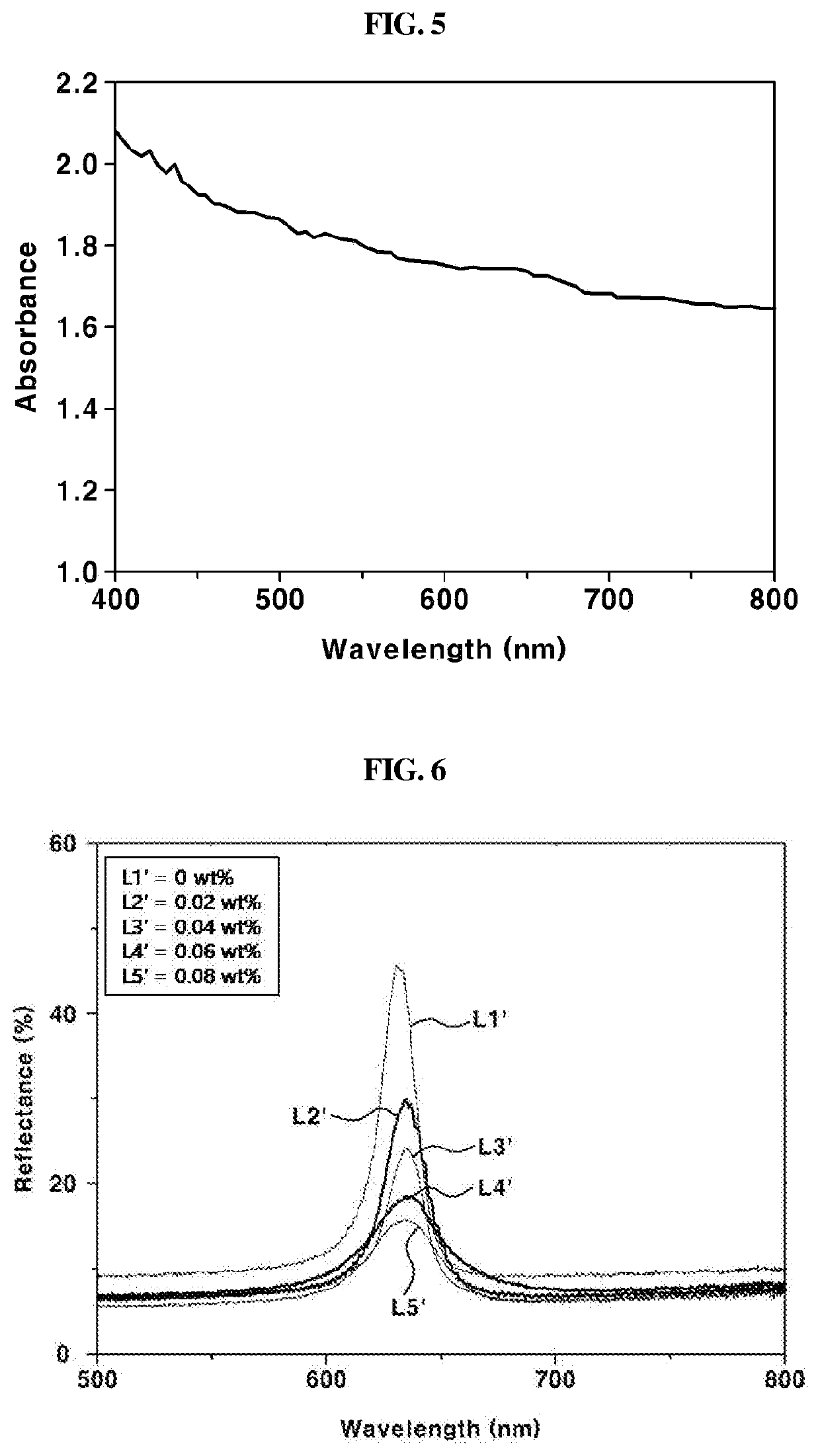
[0104]A photonic crystal structure and a porous structure were manufactured in the same manner as in Example 1, with the exception that the average particle size of the silica particles was adjusted to 202 nm, and carbon black having an average particle size of 24 nm was added in an amount of 0.02 wt %, in lieu of the melanin nanoparticles.
[0105](2) Formation of Photonic Crystal Structure (Film)
[0106]The photonic crystal ink composition was made to penetrate between two glass plates having a 50 μm gap therebetween, irradiated with UV light, and cured, thus manufacturing a film layer.
[0107](3) Formation of Porous Structure (Film)
[0108]The photonic crystal structure (film) was treated with a hydrofluoric acid solution having a concentration of 2 vol % for about 12 hours, washed with water, and dried, thus manufacturing a porous structure (film).
PUM
| Property | Measurement | Unit |
|---|---|---|
| diameter | aaaaa | aaaaa |
| diameter | aaaaa | aaaaa |
| diameter | aaaaa | aaaaa |
Abstract
Description
Claims
Application Information


