Load driving circuit
- Summary
- Abstract
- Description
- Claims
- Application Information
AI Technical Summary
Benefits of technology
Problems solved by technology
Method used
Image

Examples
first example
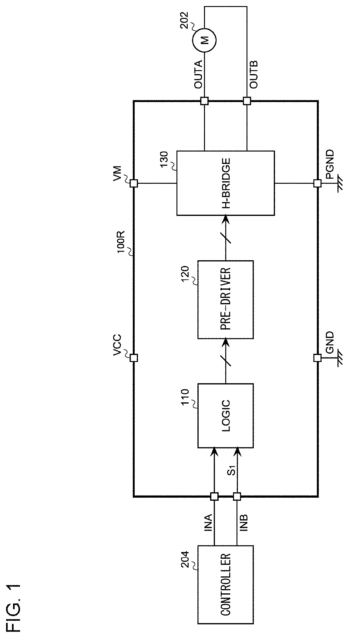
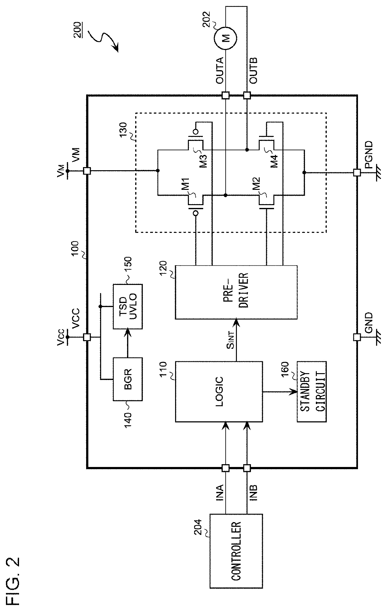
[0040]FIG. 2 is a circuit diagram showing a system 200 including a driving circuit 100 according to a first example. The driving circuit 100 includes two control input pins INA and INB. Two control input signals are supplied from an external controller 204 to the two control input pins INA and INB, respectively. The driving circuit 100 drives a load (e.g., a motor 202) coupled to the two output terminals OUTA and OUTB.
[0041]The driving circuit 100 includes a logic circuit 110, a pre-driver 120, an H-bridge circuit 130, a BGR (bandgap reference) circuit 140, a protection circuit 150, and a standby circuit 160, which are housed in a single package. The driving circuit 100 may be configured as a function IC integrated on a single semiconductor substrate. Alternatively, the H-bridge circuit 130 may be integrated on a different chip from that on which the other blocks (110, 120, 140, 150, and 160) are integrated.
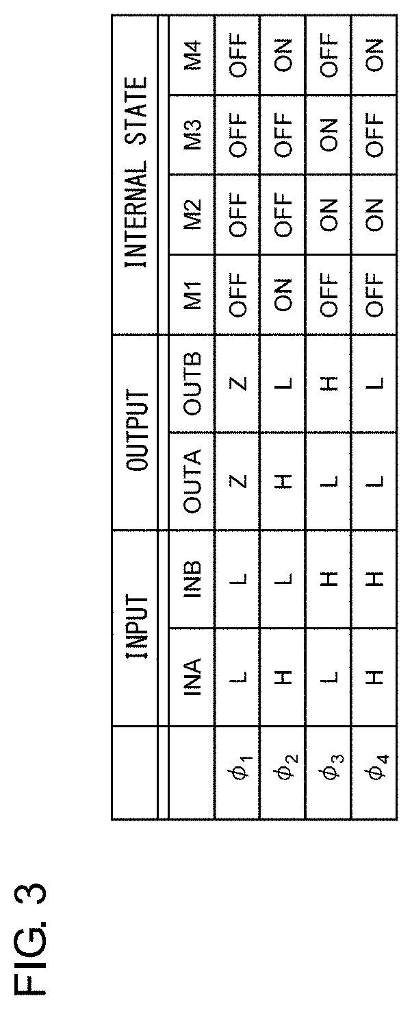
[0042]The H-bridge circuit 130 can be set to one from among four states ϕ1 t...
second example
[0062]FIG. 5 is a circuit diagram showing a system 200A including a driving circuit 100A according to a second example. The driving circuit 100A includes a PWM (Pulse Width Modulation) circuit 170 configured to switch on and off a driving signal. A shunt resistor Rs is provided on a path of a driving current, and specifically, between a PGND pin and an external ground. A voltage drop (current detection signal) Vs occurs across the shunt resistor Rs according to the driving current that flows through the motor 202. The shunt resistor Rs may be built into the driving circuit 100A.
[0063]The PWM circuit 170 is configured as a pulse-by-pulse current limiting circuit. The PWM circuit 170 generates a PWM signal SPWM based on the current detection signal Vs. The PWM circuit 170 operates in synchronization with a clock generated by an oscillator 172. For example, the PWM circuit 170 switches the PWM signal SPWM to a first level (e.g., high level) in response to a positive edge of the clock C...
third example
[0066]FIG. 6 is a circuit diagram showing a system 200B including a driving circuit 100B according to a third example. The driving circuit 100B includes a single control pin IN. The control pin receives the input of a control input signal IN configured as a high / low binary signal. The logic circuit 110 switches the state of the bridge circuit 130 in response to transition of the state of the control input pin IN. Furthermore, when the control input pin IN continues in a predetermined state for a predetermined period of time, the standby circuit 160 switches the driving circuit 100B to the standby state.
[0067]FIG. 7A through FIG. 7C are diagrams showing several examples of the correspondence between the state of the control input pin IN of the driving circuit 100B shown in FIG. 6 and the internal state and the output state of the driving circuit 100B. This arrangement allows the H-bridge circuit 130 to be switched between the following two states ϕ1 and ϕ2.
[0068]ϕ1 OUT1=L, OUT2=H
[006...
PUM
 Abstract
Description
Claims
Application Information
 - R&D Engineer
- R&D Manager
- IP Professional
- Industry Leading Data Capabilities
- Powerful AI technology
- Patent DNA Extraction
Browse by: Latest US Patents, China's latest patents, Technical Efficacy Thesaurus, Application Domain, Technology Topic.
© 2024 PatSnap. All rights reserved.Legal|Privacy policy|Modern Slavery Act Transparency Statement|Sitemap