Fingerprint sensor module comprising a fingerprint sensor device and a substrate connected to the sensor device

a fingerprint sensor and fingerprint technology, applied in the field of fingerprint sensor modules, can solve the problems of reducing the accuracy of the sensing device, reducing the connection distance between the sensing elements and the sensing surface of the fingerprint sensor module, and reducing the connection distance. the effect of the connection complexity

Active Publication Date: 2020-01-30
FINGERPRINT CARDS ANACATUM IP AB
View PDF0 Cites 5 Cited by
  • Summary
  • Abstract
  • Description
  • Claims
  • Application Information

AI Technical Summary

Benefits of technology

The patent text describes a fingerprint sensor module that is mounted in an electronic device. The module has a substrate that connects to a trench on the edge of the device. This substrate helps to connect the fingerprint sensor to other parts of the device and also allows for additional components to be added. The substrate is designed to be thinner than the depth of the trench, which prevents it from sticking out and getting in the way. This design ensures that the fingerprint sensor is positioned close enough to the surface of the device for accurate fingerprint reading.

Problems solved by technology

Accordingly, protruding wire bonds introduce constraints in the assembly and design of a fingerprint sensor.
However, a thicker coating result in a weaker capacitive coupling between a finger placed on the surface and a sensing element located under the coating, which leads to a reduced accuracy of the sensing device.
Another solution would be to connect the fingerprint sensor device to the substrate by means of through-silicon-via connections (TSVs) which does not add an extra layer of material on top of the pixels but where the manufacturing process instead is complicated, making it expensive and difficult to optimize.
In addition, using the TSV solution requires thin silicon, making the TSV package more prone to package warpage.

Method used


Image

  • Fingerprint sensor module comprising a fingerprint sensor device and a substrate connected to the sensor device
  • Fingerprint sensor module comprising a fingerprint sensor device and a substrate connected to the sensor device
  • Fingerprint sensor module comprising a fingerprint sensor device and a substrate connected to the sensor device

Examples


Embodiment Construction

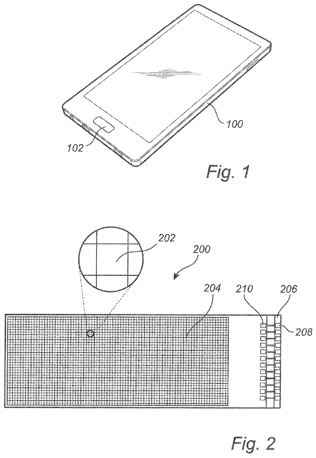
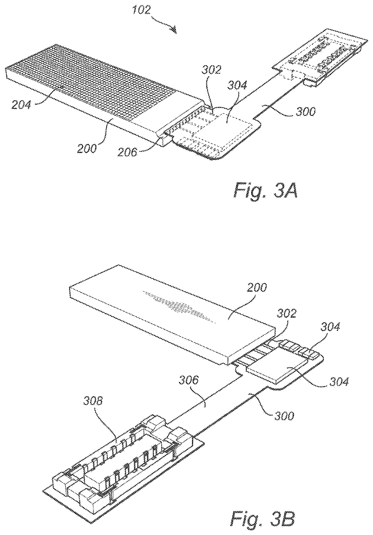
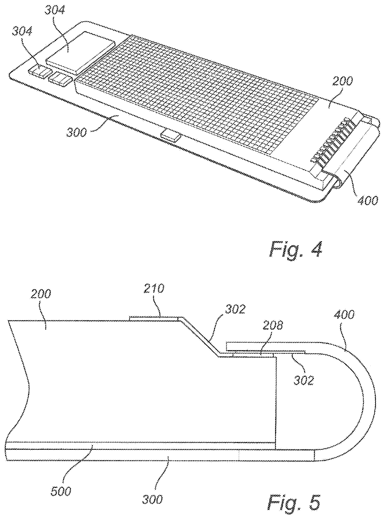
[0038]In the present detailed description, various embodiments of the sensor module and method according to the present invention will be described. Embodiments of the present invention are mainly described with reference to a capacitive fingerprint sensing device arranged in a smartphone. However, it should be noted that the present invention is applicable for any type of fingerprint sensor. The fingerprint sensor device may for example be an active or passive capacitive device, an ultrasonic or an optical device.

[0039]FIG. 1 schematically illustrates a smartphone 100 comprising a fingerprint sensor module 102 according to an example embodiment of the present invention. The fingerprint sensor module 102 may, for example, be used for unlocking the smartphone 100 and / or for authorizing transactions carried out using the smartphone. A fingerprint sensing module according to various embodiments of the invention may also be used in other electronic devices, such as tablet computers, lap...


PUM

PropertyMeasurementUnit
thicknessaaaaaaaaaa
thicknessaaaaaaaaaa
electrically conductiveaaaaaaaaaa

Abstract

There is provided a fingerprint sensor module comprising: a fingerprint sensor device comprising a plurality of sensing elements for acquiring an image of a finger placed on a sensing surface of the sensor module. The sensor device comprises a trench at an edge of the fingerprint sensor device, the trench comprising electrically conductive connection pads for connecting the sensor device to external circuitry. The module further comprises a substrate comprising an electrically conductive trace and an electric component arranged on the substrate and in electrical contact with the conductive trace. The substrate is electrically and mechanically connected to the edge trench such that an electrical connection is formed between the sensor device and the electrical component of the substrate via the conductive trace. There is also provided a method for manufacturing the described module.

Description

FIELD OF THE INVENTION[0001]The present invention relates to a fingerprint sensor module and to a method for manufacturing a fingerprint sensor module comprising a fingerprint sensor device and a substrate connected to the sensor device.BACKGROUND OF THE INVENTION[0002]As the development of biometric devices for identity verification, and in particular of fingerprint sensing devices, has lead to devices which are made smaller, cheaper and more energy efficient, the possible applications for such devices are increasing. Fingerprint sensing in particular has been adopted in more and more applications such as consumer electronic devices and smart cards due to small form factor, relatively beneficial cost / performance factor and high user acceptance.[0003]Capacitive fingerprint sensing devices, built based on CMOS technology for providing the fingerprint sensing elements and auxiliary logic circuitry, are increasingly popular as such sensing devices can be made both small and energy effi...

Claims


Application Information

Patent Timeline
Patent Type & Authority Applications(United States)
IPC IPC(8): G06K9/00H01L23/12H01L23/31G06V40/13
CPCG06K9/0002G06K9/00053H01L23/12H01L23/31G06V40/1306G06V40/1329
Inventor JULIAN, ROGELIO
Owner FINGERPRINT CARDS ANACATUM IP AB
Why Eureka
Try Eureka