
Control buffer for reducing EMI and source driver including the same

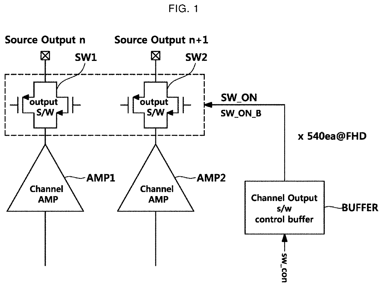
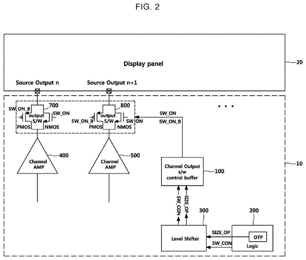
a control buffer and emi technology, applied in logic circuit coupling/interface arrangement, pulse technique, instruments, etc., can solve the problems of increasing electromagnetic interference, reducing emi, and high level of electromagnetic interference, so as to reduce the load of the display panel, reduce and increase the size of the control buffer

Active Publication Date: 2020-01-30
MAGNACHIP SEMICONDUCTOR LTD
View PDF10 Cites 0 Cited by
  • Summary
  • Abstract
  • Description
  • Claims
  • Application Information

AI Technical Summary

Benefits of technology

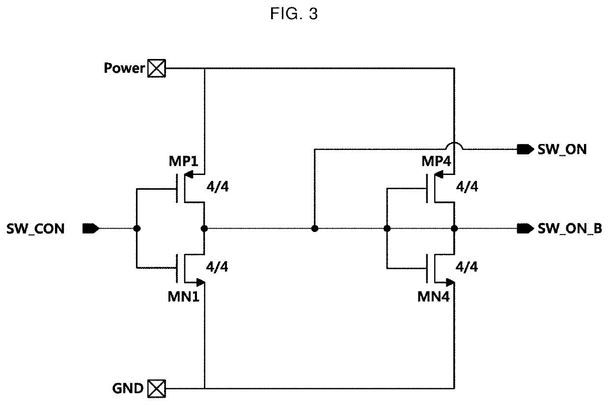
The control buffer is a component used in electronic devices to reduce electromagnetic interference (EMI) in switch signals. The text states that when the size of the control buffer decreases, EMI can be reduced. Conversely, when the load (the amount of work) on the display panel increases, the size of the control buffer may need to increase to handle the additional load. The text also mentions that when the load on the display panel decreases, the size of the control buffer may decrease to handle the reduced load.

Problems solved by technology

As semiconductors become more integrated, electromagnetic interference (EMI) phenomena increase.
Thus, reducing EMI is an important issue in semiconductor and IC design.
Such an approach may induce the occurrence of a high level of electromagnetic interference (EMI), which may affect display image quality.
A high level of EMI may also affect receiver sensitivity for mobile phones adversely.
As the load of the display panel increases, the size of the control buffer may increase, and as the load of the display panel decreases, the size of the control buffer may decrease.

Method used


Image

  • Control buffer for reducing EMI and source driver including the same
  • Control buffer for reducing EMI and source driver including the same
  • Control buffer for reducing EMI and source driver including the same

Examples


Embodiment Construction

[0042]The following detailed description is provided to assist the reader in gaining a comprehensive understanding of the methods, apparatuses, and / or systems described herein. However, various changes, modifications, and equivalents of the methods, apparatuses, and / or systems described herein will be apparent after an understanding of the disclosure of this application. For example, the sequences of operations described herein are merely examples, and are not limited to those set forth herein, but may be changed as will be apparent after an understanding of the disclosure of this application, with the exception of operations necessarily occurring in a certain order. Also, descriptions of features that are known in the art may be omitted for increased clarity and conciseness.

[0043]The features described herein may be embodied in different forms, and are not to be construed as being limited to the examples described herein. Rather, the examples described herein have been provided mer...


PUM


Abstract

A control buffer in a source driver includes a first CMOS inverter configured to output a switch signal to control turning on and off of a switch, and a first tri-state inverter that is connected to the first CMOS inverter and configured to selectively adjust a size of the control buffer, wherein a slew rate of the switch signal is adjusted depending on the size of the control buffer.

Description

CROSS-REFERENCE TO RELATED APPLICATIONS[0001]This application claims the benefit under 35 USC 119(a) of Korean Patent Application No. 10-2018-0088027 filed on Jul. 27, 2018 in the Korean Intellectual Property Office, the entire disclosure of which is incorporated herein by reference for all purposes.BACKGROUND1. Field[0002]The following description relates to a control buffer included in a source driver. The following description also relates to a control buffer that is capable of reducing electromagnetic interference (EMI). Furthermore, the following description relates to a source driver including such a control buffer.2. Description of Related Art[0003]Integrated Circuits (ICs) in which large numbers of transistors are included on one semiconductor chip are referred to as Large Scale Integration (LSI), very LSI, or ultra LSI ICs depending on the density of integration of transistors on such ICs.[0004]As semiconductors become more integrated, electromagnetic interference (EMI) phe...

Claims


Application Information

Patent Timeline
Patent Type & Authority Applications(United States)
IPC IPC(8): G09G5/00
CPCG09G2310/0291G09G5/003H03K19/017509H03K19/018521H03K19/00315H03K19/00361G09G3/20G09G2310/0275G09G2330/06G09G2310/08G09G2310/06G09G2310/027H03K19/09425
Inventor SEONG, EUN KYUKIM, HYOUNG KYU
Owner MAGNACHIP SEMICONDUCTOR LTD
Learn More