Multilayer ceramic electronic component

a technology of electronic components and ceramics, applied in the direction of fixed capacitor details, stacked capacitors, fixed capacitor terminals, etc., can solve the problems of easy breakage of plating film, easy breakage of base electrodes and plating films, and easy breakage of plating films in holding elements, etc., to achieve low profile

Active Publication Date: 2020-01-30
TDK CORPARATION
View PDF0 Cites 2 Cited by
  • Summary
  • Abstract
  • Description
  • Claims
  • Application Information

AI Technical Summary

Benefits of technology

[0006]The present invention has been achieved under such circumstances. It is an object of the invention to...

Problems solved by technology

In any case, when the terminal electrodes are formed on the element body, the base electrodes and the plating film are hard to be formed if the element body is not thick.
That is, when the element body is thin, it easily gets broken in holding the element body by t...

Method used


Image

  • Multilayer ceramic electronic component
  • Multilayer ceramic electronic component
  • Multilayer ceramic electronic component

Examples


first embodiment

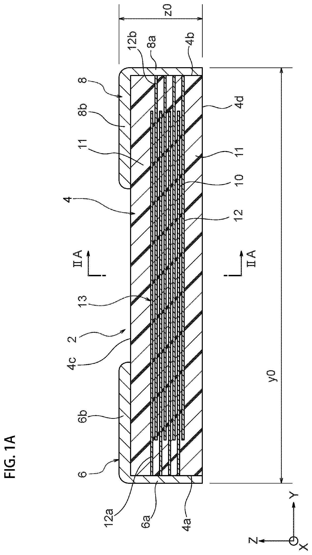
[0045]As an embodiment of a multilayer ceramic electronic component according to the present embodiment, a multilayer ceramic capacitor is described.

[0046]As shown in FIG. 1A, a multilayer ceramic capacitor 2 according to the present embodiment includes an element body 4, a first terminal electrode 6, and a second terminal electrode 8. The element body 4 includes inner dielectric layers (insulation layers) 10 and internal electrode layers 12 in substantially parallel to the plane including the X-axis and the Y-axis. The internal electrode layers 12 are alternately laminated along the Z-axis direction between the inner dielectric layers 10. Here, “substantially parallel” means that most part is parallel, but there may be a part that is not slightly parallel. The internal electrode layers 12 and the inner dielectric layers 10 may slightly be uneven or inclined.

[0047]An interior region 13 is a region where the inner dielectric layers 10 and the internal electrode layers 12 are alternat...

second embodiment

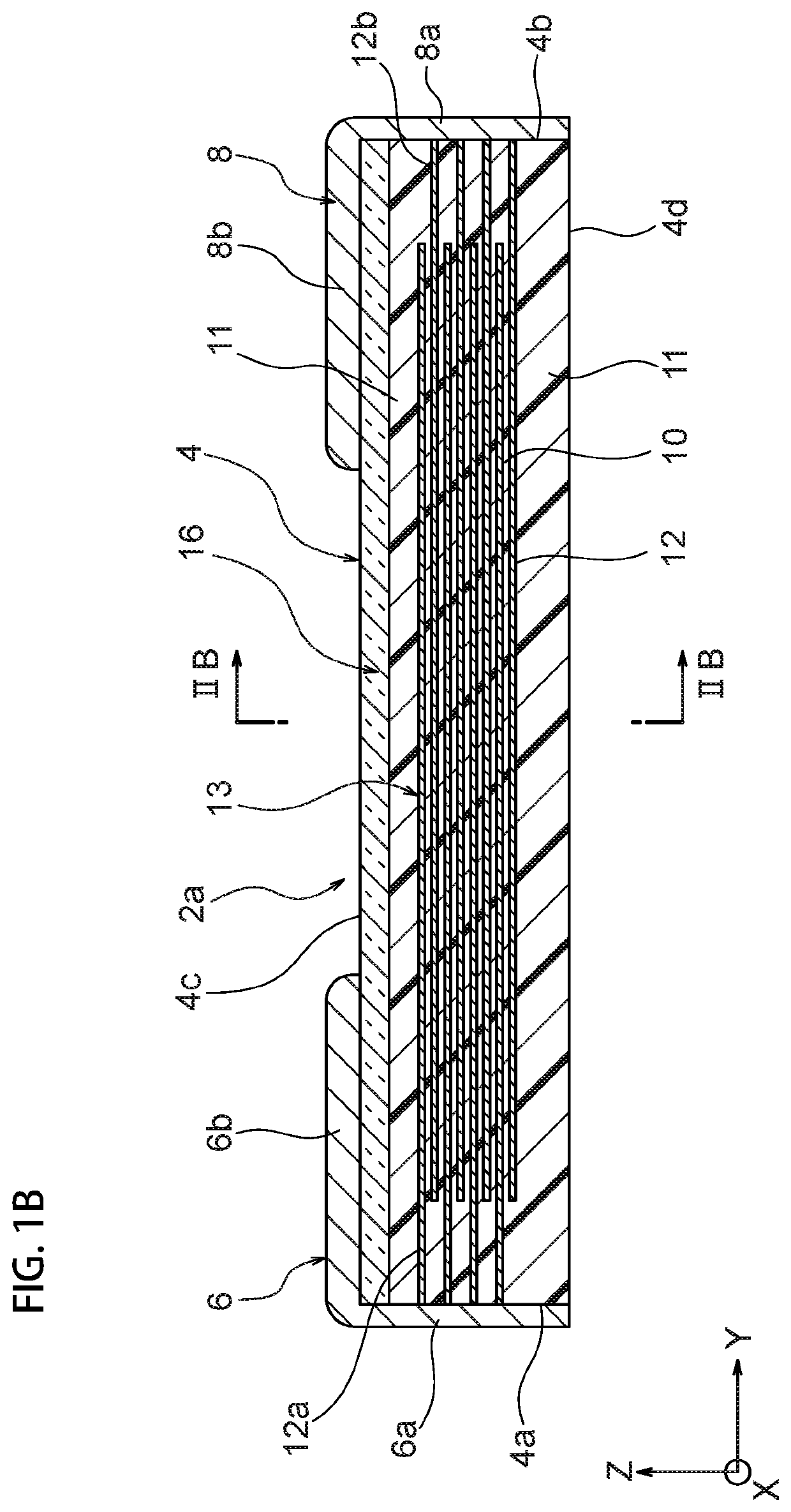
[0089]Except for the following matters, as shown in FIG. 1B and FIG. 2B, a multilayer ceramic capacitor 2a according to the present embodiment is similar to the multilayer ceramic capacitor 2 according to First Embodiment. In the multilayer ceramic capacitor 2a, the upper surface 4c (or the lower surface 4d) of the element body 4 includes a reinforcement layer 16 made of a material that is stronger than the inner dielectric layers 10, and the outer surface of the reinforcement layer 16 defines the upper surface 4c (or the lower surface 4d) of the element body 4.

[0090]After the element body 4 is formed similarly to First Embodiment, the reinforcement layer 16 is formed on the upper surface 4c (or the lower surface 4d) of the element body 4 before the terminal electrodes 6 and 8 are formed. The reinforcement layer 16 is not limited and is glass, alumina based composite material, zirconia based composite material, polyimide resin, epoxy resin, aramid fiber, fiber reinforced plastic, or...

third embodiment

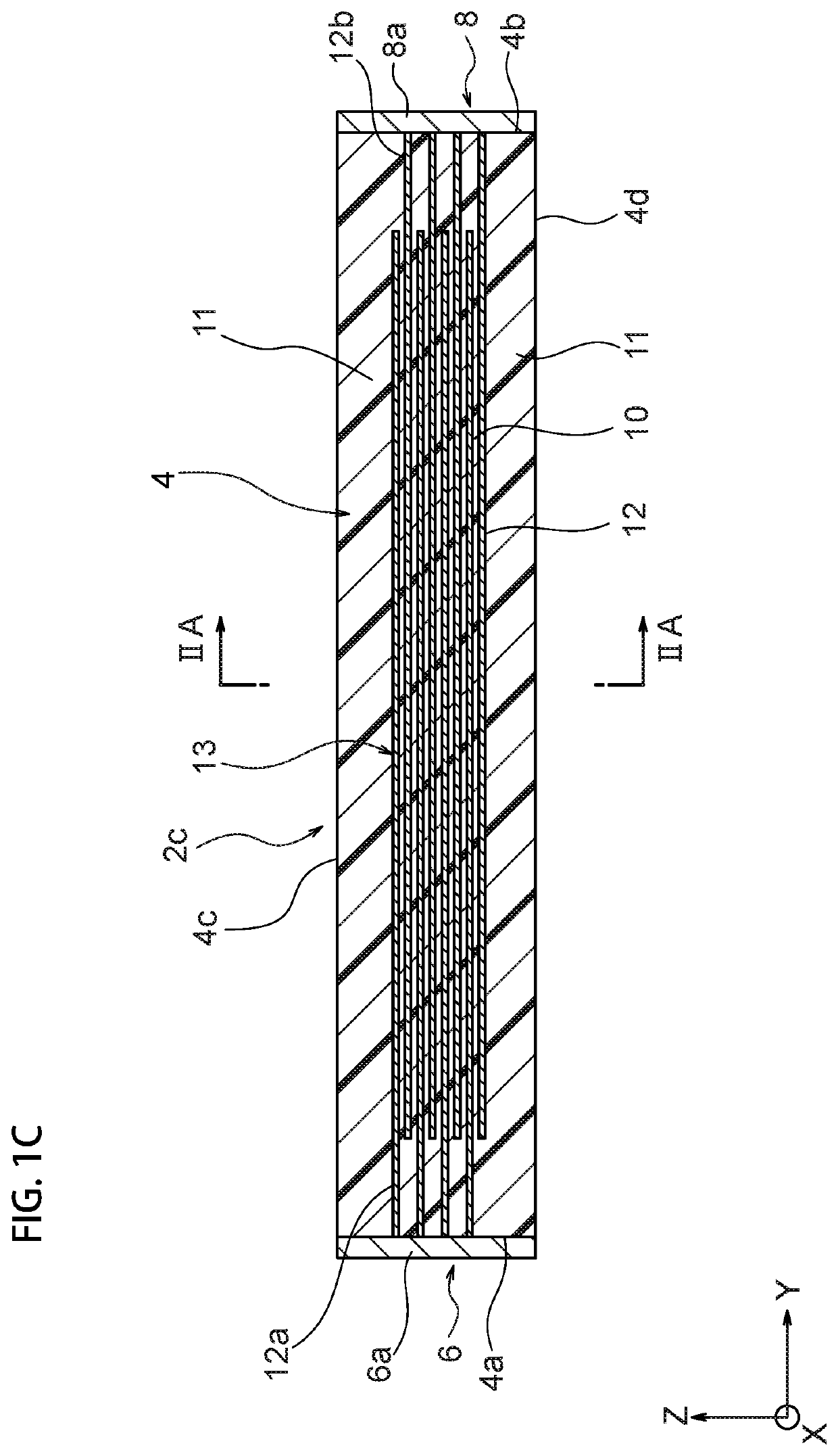
[0103]Except for the following matters, as shown in FIG. 2C, a multilayer ceramic capacitor 2b according to the present embodiment is similar to the multilayer ceramic capacitor 2a according to Second Embodiment. In the multilayer ceramic capacitor 2b, the reinforcement layer 16 has lateral cover parts 16a covering the side surfaces 4e of the element body 4. The lateral cover parts 16a are formed continuously with the reinforcement layer 16 of Second Embodiment. This structure further improves the strength of the multilayer ceramic capacitor.

[0104]Incidentally, FIG. 2C illustrates that each of the lateral cover parts 16a constitutes only a part of the side surface 4e of the side-gap region 14, but may constitute the whole of the side-gap region 14. That is, the lateral cover parts 16a may be in contact with the ends of the internal electrode layers 12 in the X-axis direction.

[0105]The present invention is not limited to the above-mentioned embodiments and may variously be changed wi...


PUM

PropertyMeasurementUnit
Elasticityaaaaaaaaaa
Thermal expansion coefficientaaaaaaaaaa

Abstract

A multilayer ceramic electronic component includes an element body and a terminal electrode. The element body includes internal electrode layers and insulation layers alternately laminated in a lamination direction. The terminal electrode is formed on an outer surface of the element body to be contacted and connected with the internal electrode layers. The terminal electrode includes an end-side electrode part and an upper-side electrode part. The end-side electrode part covers a leading end of the element body where the internal electrode layers are led. The upper-side electrode part is formed on a part of an upper surface of the element body and continues to the end-side electrode part. The terminal electrode is not substantially formed on a lower surface of the element body located on the other side of the upper surface along the lamination direction.

Description

BACKGROUND OF THE INVENTION[0001]The present invention relates to a multilayer ceramic electronic component used as, for example, a multilayer ceramic capacitor and specifically relates to a multilayer ceramic electronic component capable of being thin.[0002]For example, as shown in Patent Document 1, it is normal for conventional multilayer ceramic capacitors that terminal electrodes are arranged on both ends of an element body in its longitudinal direction, and that each of the terminal electrodes includes an end-side electrode part of the element body and cover electrode parts covering upper and lower surfaces of the element body.[0003]Base electrodes of the terminal electrodes are formed by immersing the ends of the element body into a solution containing conductive particles. In the immersion, multiple element bodies are respectively put into multiple holding holes formed on a holding plate, and ends of the element bodies are immersed into the solution per each side. After that...

Claims


Application Information

Patent Timeline
IPC IPC(8): H01G4/232H01G4/258H01G4/30
CPCH01G4/30H01G4/232H01G4/224H01G4/12H01G2/106H01G2/06H01G4/258
Inventor SAKURAI, TOSHIOTANAKA, HIROBUMIOKAI, KEISUKEIWANAGA, DAISUKENAKATA, HISASHISIHBASAKI, TOMOYA
Owner TDK CORPARATION
Why Eureka
Try Eureka