
Method for patterning a semiconductor structure

a semiconductor structure and patterning technology, applied in the field of semiconductor manufacturing, can solve the problems of pattern deformation, difficult control of thickness and uniformity, etc., and achieve the effect of improving the loading

Active Publication Date: 2020-01-30
UNITED MICROELECTRONICS CORP +1
View PDF0 Cites 1 Cited by
  • Summary
  • Abstract
  • Description
  • Claims
  • Application Information

AI Technical Summary

Benefits of technology

This approach improves the SADP process by maintaining pattern integrity and preventing over-etching, allowing for precise pattern transfer without deforming the semiconductor substrate, thus overcoming the loading effect caused by pattern density differences.

Problems solved by technology

However, some difficulties have been encountered when applying the SADP process to form the array pattern of a DRAM device because the dramatic pattern density differences between the array region and the peripheral region may cause a loading effect to the SADP process, making it difficult to control the thickness and uniformity of the material layer used in the SADP process, which may cause deformation of patterns due to insufficient thickness of the material layer or unexpected patterns and residues due to too much thickness of the material layer.

Method used


Image

  • Method for patterning a semiconductor structure
  • Method for patterning a semiconductor structure
  • Method for patterning a semiconductor structure

Examples


Embodiment Construction

[0015]To provide a better understanding of the present invention to those of ordinary skill in the art, several exemplary embodiments will be detailed as follows, with reference to the accompanying drawings using numbered elements to elaborate the contents and effects to be achieved.

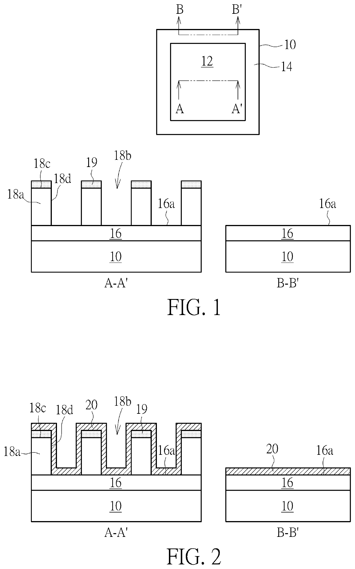
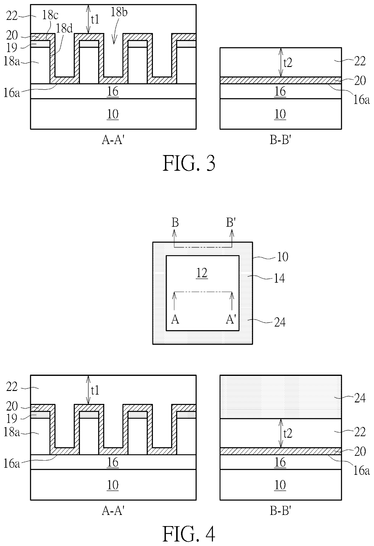
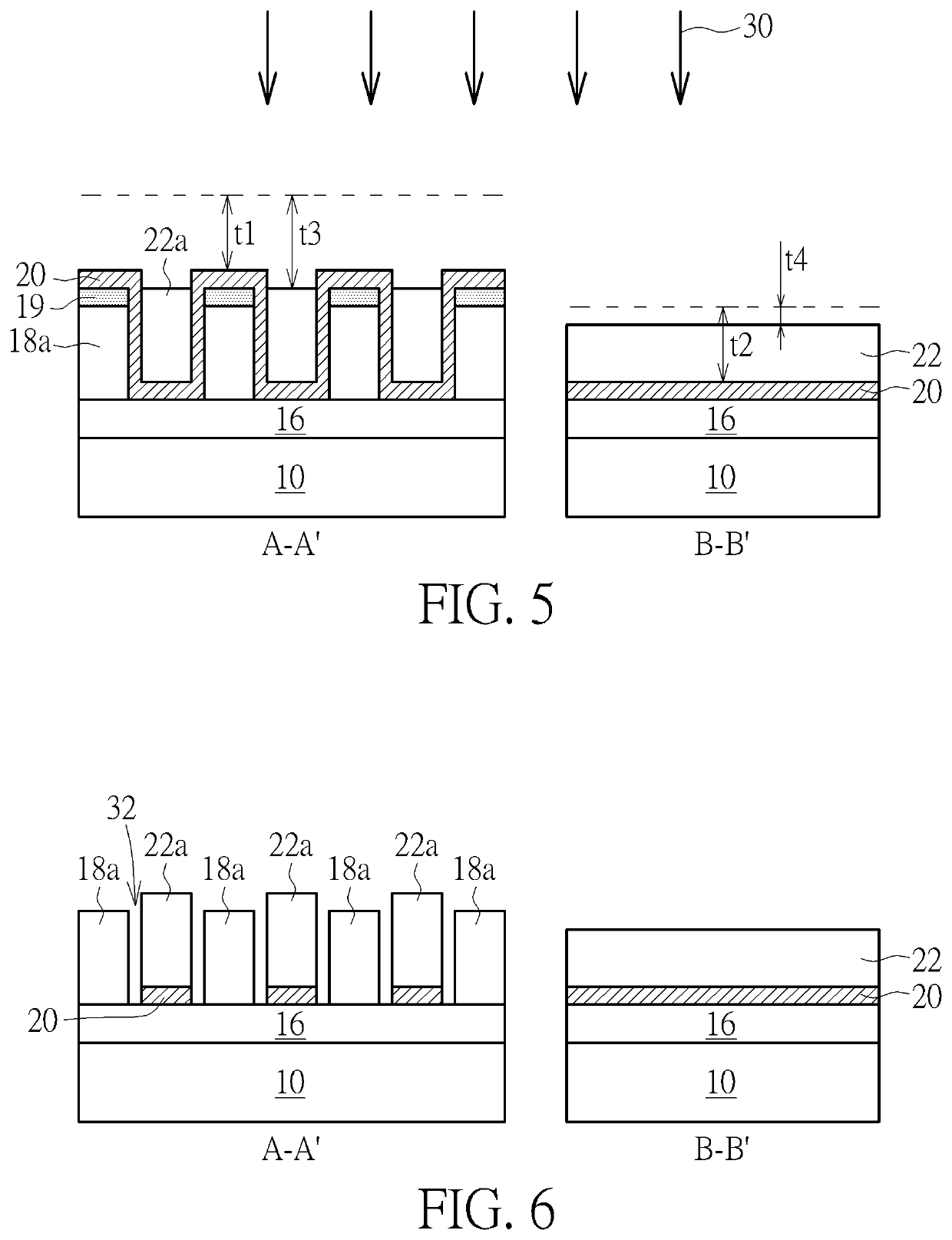
[0016]FIG. 1 to FIG. 7 illustrate the steps for patterning a semiconductor structure according to a first embodiment of the present invention. The upper portions of FIG. 1 and FIG. 4 are top views of the semiconductor structure. The lower portions of FIG. 1 and FIG. 4 are cross-sectional views of the semiconductor structure along line A-A′ in the array region 12 and line B-B′ in the peripheral region 14 as shown in the top views. FIG. 2, FIG. 3, FIG. 5, FIG. 6 and FIG. 7 are cross-sectional views taken along line A-A′ and line B-B′ illustrating the cross-sectional structure of the semiconductor structures in different process steps.

[0017]Please refer to FIG. 1. A substrate 10 is provided. The substrate 1...


PUM


Abstract

A method for patterning a semiconductor structure is provided, including forming an additional third material layer on a thinner portion of a second material layer to be an etching buffer layer. The removed thickness of the thinner portion of the second material layer covered by the third material layer during an etching back process is therefore reduced.

Description

Cross Reference To Related Applications[0001]This patent application is a divisional application of and claims priority to U.S. patent application Ser. No. 15 / 968,680 filed on May 1, 2018, and the entire content of which is hereby incorporated by reference.BACKGROUND OF THE INVENTION1. Field of the Invention[0002]The invention relates to semiconductor manufacturing, and more particularly to a method for patterning a semiconductor structure.2. Description of the Prior Art[0003]Dynamic random access memory (DRAM) is one kind of volatile memory. A DRAM device usually includes an array region comprising plural memory cells and a peripheral region comprising control circuit. The control circuits in the peripheral region may address each of the memory cells in the array region by plural columns of word lines and plural rows of bit lines traversing the array region and electrically connected to each of the memory cells to perform reading, writing or erasing data. In advanced semiconductor ...

Claims


Application Information

Patent Timeline
Patent Type & Authority Applications(United States)
IPC IPC(8): H01L21/033H01L21/02H01L27/108H01L21/3105H01L21/027H10B12/00
CPCH01L21/31111H01L21/0271H01L21/31133H01L21/0337H01L21/02164H01L21/31058H01L27/10897H01L27/10894H01L21/0217H01L21/3086H10B12/09H10B12/50
Inventor FENG, LI-WEIWEI, MING-TELIN, YU-CHIEHWANG, YING-CHIAOHO, CHIEN-TING
Owner UNITED MICROELECTRONICS CORP
Features
  • Generate Ideas
  • Intellectual Property
  • Life Sciences
  • Materials
  • Tech Scout
  • Unparalleled Data Quality
  • Higher Quality Content
  • 60% Fewer Hallucinations
Learn More