Package structure and bonding method thereof

a packaging structure and bonding method technology, applied in the field of packaging technique, can solve the problems of high resistance at the contact point, complex manufacturing process, and separation of the bonding surface, and achieve the effect of favorable bonding strength and bonding quality

Active Publication Date: 2020-02-06
UNIMICRON TECH CORP
View PDF3 Cites 4 Cited by
  • Summary
  • Abstract
  • Description
  • Claims
  • Application Information

AI Technical Summary

Benefits of technology

[0005]The invention provides a package structure, which is suitable for a low temperature bonding assembly and has favorable bonding strength and bonding quality.
[0006]The invention provides a bonding method of a package structure, which is suitable for reducing process requirements, reducing manufacturing cost and improving quality and reliability of the package structure.
[0017]Based on the above, with the package structure and the bonding method thereof according to the invention, the adhesive layer may be disposed between the first substrate and the second substrate before press-fitting the first substrate to the second substrate. After bonding, the adhesive layer may fill in the gaps between the first substrate and the second substrate and fill in the gaps between the conductive pillars. Accordingly, sealing protection, favorable bonding strength and bonding quality may be achieved under the premise of refining the contact points. Moreover, during bonding, because a stress concentrator may be produced between the conductive pillar and the pad in contact, process temperature and pressure for bonding may be effectively reduced to be suitable for the low temperature bonding assembly. In comparison with the conventional bonding technique, the bonding method of the package structure of the invention is suitable for reducing process requirements, reducing manufacturing cost and improving quality and reliability of the package structure. Further, the conductive pillars can fill in the vias and achieve favorable electrical connection with the pads to allow the package structure to provide favorable electrical property that further improves quality of the package structure.

Problems solved by technology

However, the above bonding techniques with use of a solder balls may encounter problems like bonding surface separation due to long-term fatigue, reliability issue caused by the defective solder during the manufacturing process, and relatively high resistance on contact points.
In addition, because the surface of the copper structure needs to be well cleaned for obtaining a flat surface through a chemical polishing process (CMP) before bonding, the manufacturing process is complicated so manufacturing cost cannot be reduced.
Moreover, the underfill used after bonding for reducing the size of the package structure and refining the contact points may not be able to reliably cover the contact points each time such that quality and reliability for bonding may be reduced accordingly.

Method used


Image

  • Package structure and bonding method thereof
  • Package structure and bonding method thereof
  • Package structure and bonding method thereof

Examples


Embodiment Construction

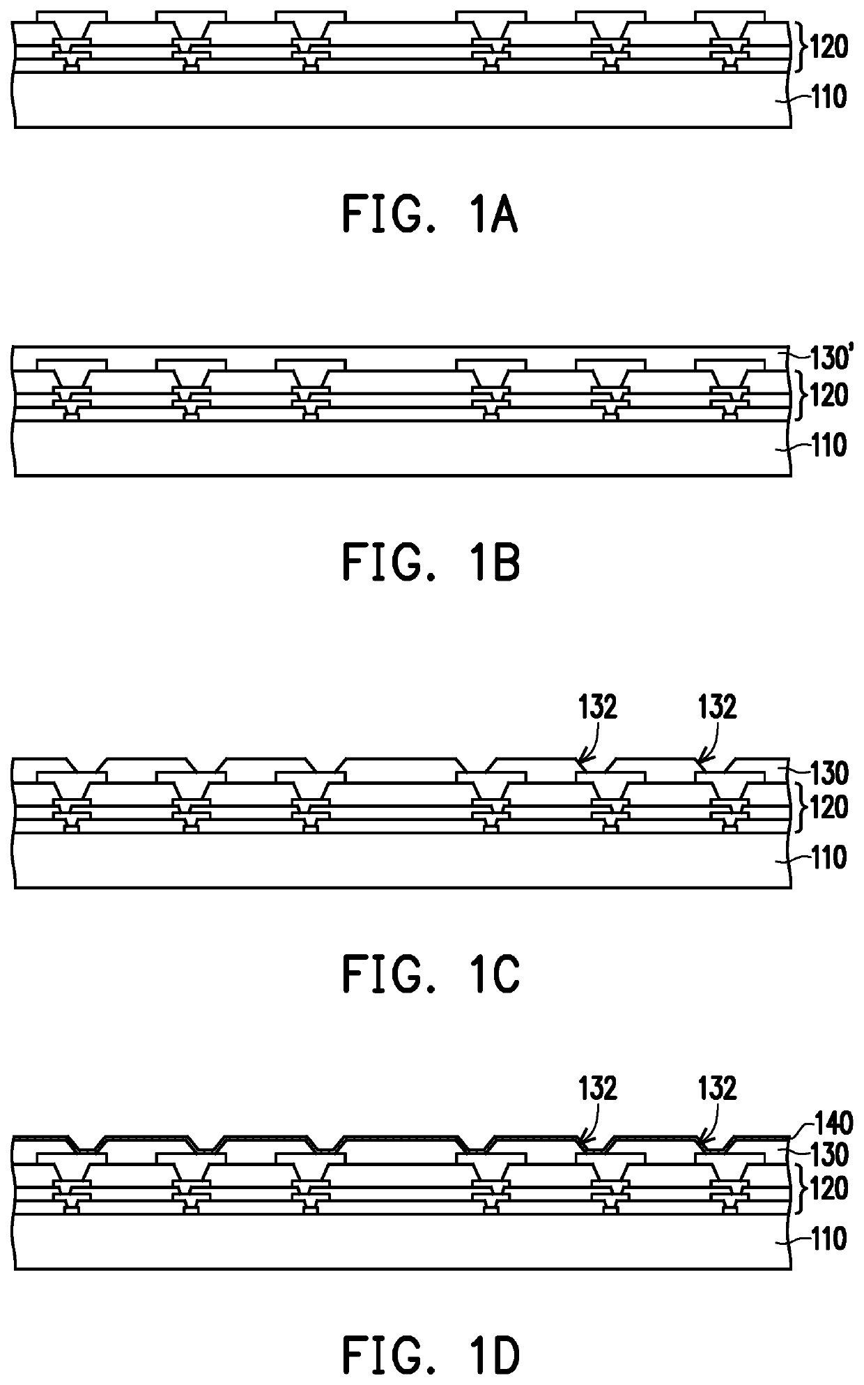
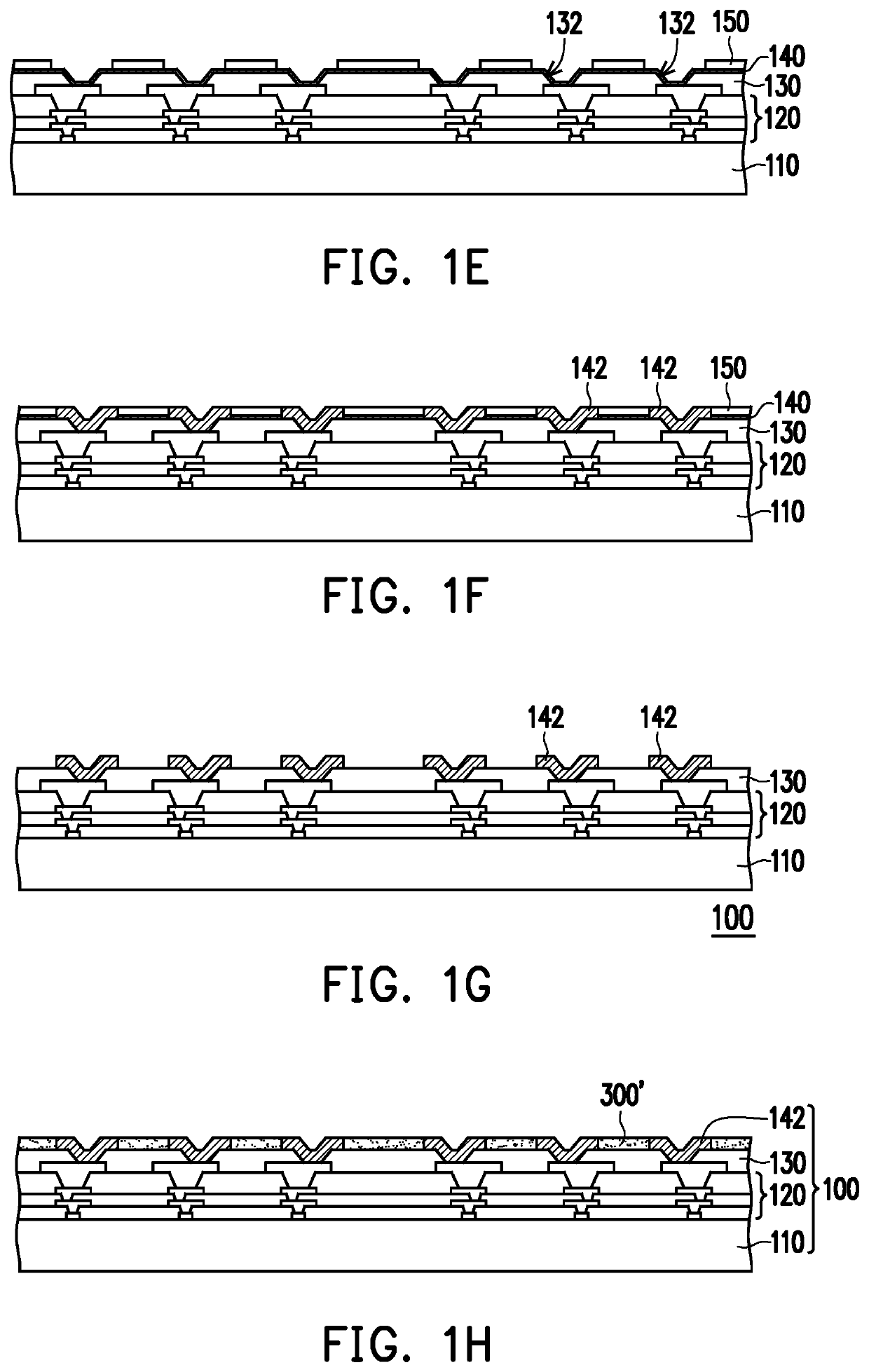
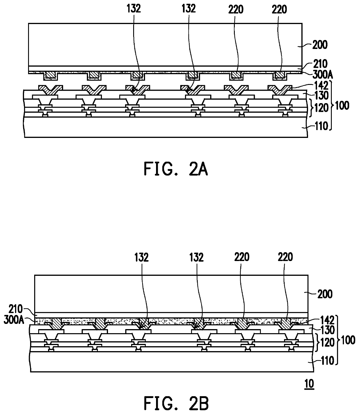
[0033]Some embodiments are provided hereinafter and described in detail with reference to the accompanied drawings. However, the embodiments provided are not intended to limit the scope of the invention. Further, the drawings are only descriptive and are not drawn to scale. For ease of explanation, the same devices below are provided with the same reference numerals.

[0034]Moreover, terms such as “first” and “second” used herein do not represent sequence or order, and it should be understood that they are only for differentiating devices or operations having the same technical terms.

[0035]Furthermore, terms such as “contain”, “include”, and “have” used herein are all open terms, i.e., contains, but not limited to.

[0036]In addition, terms such as “contacted”, “connected”, and “bonded” used herein refer to a direction contact or indirect contact through other film layers unless otherwise stated.

[0037]FIG. 1A to FIG. 1H are cross-sectional views illustrating a manufacturing process of a...


PUM

PropertyMeasurementUnit
pressureaaaaaaaaaa
bonding temperatureaaaaaaaaaa
conductiveaaaaaaaaaa

Abstract

A package structure includes a first substrate, a second substrate, a plurality of conductive pillars and an adhesive layer. The first substrate includes a plurality of vias and a plurality of pads. The pads are disposed on the first substrate, and fill in the vias. The second substrate is disposed opposite to the first substrate. Each conductive pillar electrically connects each pad and the second substrate, and the adhesive layer fills in the gaps between the conductive pillars. A bonding method of the package structure is also provided.

Description

CROSS REFERENCE TO RELATED APPLICATION[0001]This application claims the priority benefit of Taiwan application serial no. 107127118, filed on Aug. 3, 2018. The entirety of the above-mentioned patent application is hereby incorporated by reference herein and made a part of specification.BACKGROUNDTechnical Field[0002]The invention relates to a packaging technique, and more particularly, to a package structure and a bonding method of a package structure.Description of Related Art[0003]With the evolution of semiconductor packaging technology, different package types have been developed for semiconductor devices, such as wire bonding, flip chip or hybrid (i.e., flip chip together with wire bonding) packaging techniques. However, the above bonding techniques with use of a solder balls may encounter problems like bonding surface separation due to long-term fatigue, reliability issue caused by the defective solder during the manufacturing process, and relatively high resistance on contact ...

Claims


Application Information

Patent Timeline
Patent Type & Authority Applications(United States)
IPC IPC(8): H01L23/00H01L23/498H01L21/48
CPCH01L2224/05558H01L2224/2969H01L2224/73203H01L2224/81898H01L2924/20105H01L24/32H01L2224/16227H01L2224/16237H01L2224/9211H01L24/05H01L24/73H01L24/81H01L21/4846H01L21/481H01L24/29H01L2224/2957H01L23/49838H01L2224/32225H01L2224/02331H01L24/16H01L2224/05573H01L24/92H01L2224/8385H01L24/83H01L2224/0401H01L21/563H01L23/145H01L23/49811H01L23/49822H01L23/49833H01L24/11H01L24/13H01L24/27H01L2224/1134H01L2224/1146H01L2224/13139H01L2224/13144H01L2224/13147H01L2224/13155H01L2224/13164H01L2224/13166H01L2224/16238H01L2224/27618H01L2224/29011H01L2224/29082H01L2224/2919H01L2224/29191H01L2224/73103H01L2224/73104H01L2224/73204H01L2224/81191H01L2224/81203H01L2224/81385H01L2224/81439H01L2224/81444H01L2224/81447H01L2224/81455H01L2224/81464H01L2224/81466H01L2224/83191H01L2224/83192H01L2224/83203H01L2224/9212H01L2924/00014H01L2224/81H01L2224/83H01L2924/00012H01L2224/11H01L2224/27H01L2224/16225H01L2924/00H01L2924/013H01L2924/0715H01L2924/07025H01L2924/0665H01L2924/0635
Inventor TSENG, TZYY-JANGKO, CHENG-TAYANG, KAI-MINGCHEN, YU-HUA
Owner UNIMICRON TECH CORP
Why Eureka
Try Eureka