Display device and method of fabricating the same

a technology of a display device and a manufacturing method, which is applied in the direction of semiconductor devices, electrical equipment, basic electric elements, etc., can solve the problems of different thermal expansion coefficients of the wafer on which the leds are grown, contact failures between the leds and the semiconductor elements, etc., to reduce processing time, suppress color mixture, and avoid misalignment

Active Publication Date: 2020-02-27
LG DISPLAY CO LTD
View PDF0 Cites 15 Cited by
  • Summary
  • Abstract
  • Description
  • Claims
  • Application Information

AI Technical Summary

Benefits of technology

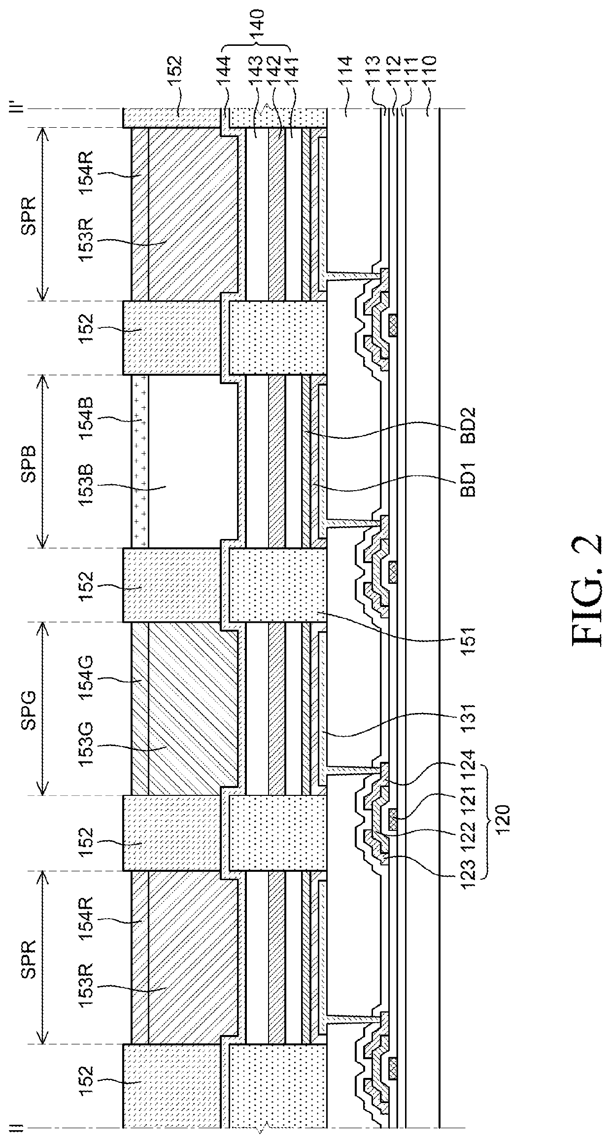
[0022]According to an exemplary embodiment of the present disclosure, it is possible to avoid misalignment due to a difference in thermal expansion coefficient between a substrate where LEDs are formed and a substrate where semiconductor elements are formed.
[0023]According to an exemplary embodiment of the present disclosure, LEDs are formed directly on the substrate where semiconductor elements are formed, so that it is possible to omit a process of transferring the LEDs onto the substrate where the semiconductor elements are formed one by one, and to reduce the processing time.
[0024]According to an exemplary embodiment of the present disclosure, it is possible to achieve a high-resolution display device by way of implementing LEDs in an ultra-small size.
[0025]According to an exemplary embodiment of the present disclosure, it is possible to suppress the color mixture between the LEDs and to improve light extraction efficiency.

Problems solved by technology

However, the thermal expansion coefficient of the wafer on which the LEDs are grown is different from that of the backplane substrate.
As a result, there is a problem in that a contact failure may occur between the LEDs and the semiconductor elements.

Method used


Image

  • Display device and method of fabricating the same
  • Display device and method of fabricating the same
  • Display device and method of fabricating the same

Examples


Embodiment Construction

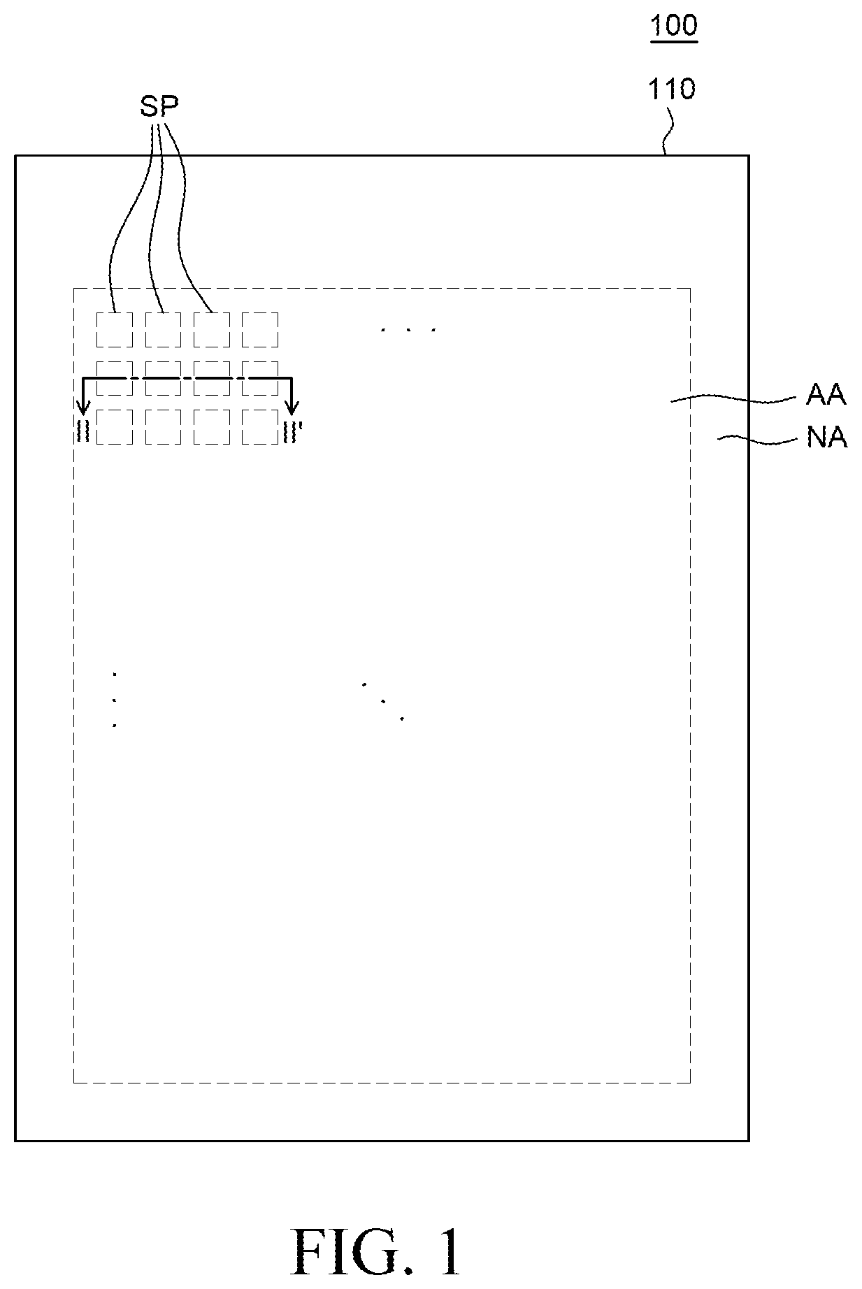
[0031]Advantages and features of the present disclosure and methods to achieve them will become apparent from the descriptions of exemplary embodiments herein below with reference to the accompanying drawings. However, the present disclosure is not limited to the exemplary embodiments disclosed herein but will be implemented in various forms. The exemplary embodiments are provided by way of example only so that those skilled in the art can fully understand the disclosures of the present disclosure and the scope of the present disclosure. Therefore, the present disclosure will be defined only by the scope of the appended claims.

[0032]The shapes, sizes, ratios, angles, numbers, and the like illustrated in the accompanying drawings for describing the exemplary embodiments of the present disclosure are merely examples, and the present disclosure is not limited thereto. Like reference numerals generally denote like elements throughout the specification. Further, in the following descript...


PUM

PropertyMeasurementUnit
sizeaaaaaaaaaa
temperatureaaaaaaaaaa
thicknessaaaaaaaaaa

Abstract

There is provided a display device. The display device includes a plurality of semiconductor elements disposed on a substrate; a plurality of LEDs disposed on the plurality of semiconductor elements and electrically connected to the plurality of semiconductor elements, respectively; and a plurality of reflectors disposed above the semiconductor elements and each located between every two of the LEDs. The plurality of LEDs may include a plurality of light-emitting layers disposed on the plurality of semiconductor elements, and a common electrode disposed on the plurality of light-emitting layers. The reflectors are disposed between the LEDs, so that light emitted from LEDs does not travel toward the side portions of the LEDs but toward the above of the substrate, thereby improving the light extraction efficiency and suppressing color mixture.

Description

CROSS-REFERENCE TO RELATED APPLICATION[0001]This application claims the priority of Korean Patent Application No. 10-2018-0098322 filed on Aug. 23, 2018, in the Korean Intellectual Property Office, the disclosure of which is incorporated herein by reference.BACKGROUNDTechnical Field[0002]The present disclosure relates to a display device and a method of fabricating the display device, and more particularly, to a display device using micro light-emitting diodes (LEDs) and a method of fabricating the display device.Description of the Related Art[0003]Display devices employed by the monitor of a computer, a TV, a mobile phone or the like includes an organic light-emitting display (OLED) that emits light by itself, and a liquid-crystal display (LCD) that requires a separate light source.[0004]Such display devices find more and more applications, including computer monitors and televisions, as well as personal portable devices. Accordingly, research is ongoing to develop display devices ...

Claims


Application Information

Patent Timeline
Patent Type & Authority Applications(United States)
IPC IPC(8): H01L27/15
CPCH01L27/156H01L33/60H01L33/62H01L33/10H01L33/38H01L33/504H01L33/58
Inventor PARK, JOONYEONGJUNG, TAEILKIM, IL-SOO
Owner LG DISPLAY CO LTD
Why Eureka
Try Eureka