Active matrix substrate and method for manufacturing the same

Active Publication Date: 2020-03-19
SHARP KK
View PDF0 Cites 6 Cited by
  • Summary
  • Abstract
  • Description
  • Claims
  • Application Information

AI Technical Summary

Benefits of technology

[0009]Moreover, according to a study by the present inventor, where TFTs of the top gate structure are used as circuit TFTs, for which a high current supplying ability is demanded, for example, if TFTs of the top gate structure are used also as pixel TFTs, the capacitance Cgs may be high in the intersection between gate bus lines and source bus lines (the details will be described later). When such a TFT substrate is used as a display device, blunting of signal waveform of signals supplied to bus lines may become significant, thereby causing brightness non-uniformi

Problems solved by technology

Moreover, in some cases, peripheral circuits such as driving circuits are monolithically (integrally) formed on a TFT substrate.
However, characteristics demanded for pixel TFTs and circuit TFTs are different from each other, and it has been difficult to selectively produce oxide semiconductor TFTs each having characteristics in accordance with the application thereof without complicating the manufacturing process

Method used


Image

  • Active matrix substrate and method for manufacturing the same
  • Active matrix substrate and method for manufacturing the same
  • Active matrix substrate and method for manufacturing the same

Examples


first embodiment

[0076]An active matrix substrate of the first embodiment will now be described with reference to the drawings. An active matrix substrate on which gate driver and source switching (Source Shared driving: SSD) circuits are formed monolithically will be described below as an example. Note that there is no limitation on the active matrix substrate of the present embodiment as long as it has a peripheral circuit that includes at least one circuit TFT monolithically formed thereon.

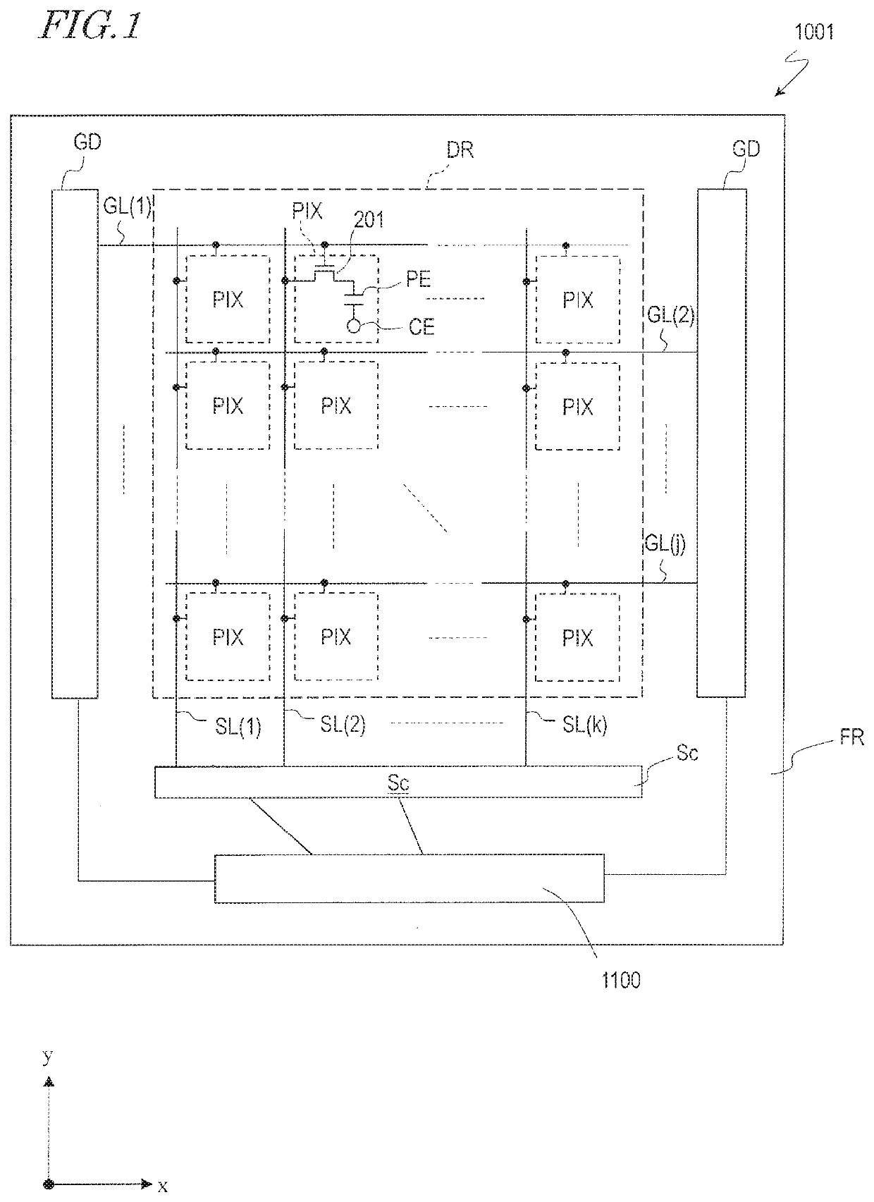
[0077]FIG. 1 is a schematic diagram showing an example of a planar structure of an active matrix substrate 1001 of the present embodiment.

[0078]The active matrix substrate 1001 includes a display region DR and a region (non-display region or bezel region) FR other than the display region DR. The display region DR includes pixel regions PIX that are arranged in a matrix pattern. The pixel region PIX (which may be referred to simply as a “pixel”) is a region corresponding to a pixel of the display device. The non...

second embodiment

[0186]An active matrix substrate of the second embodiment of the present invention will now be described with reference to the drawings.

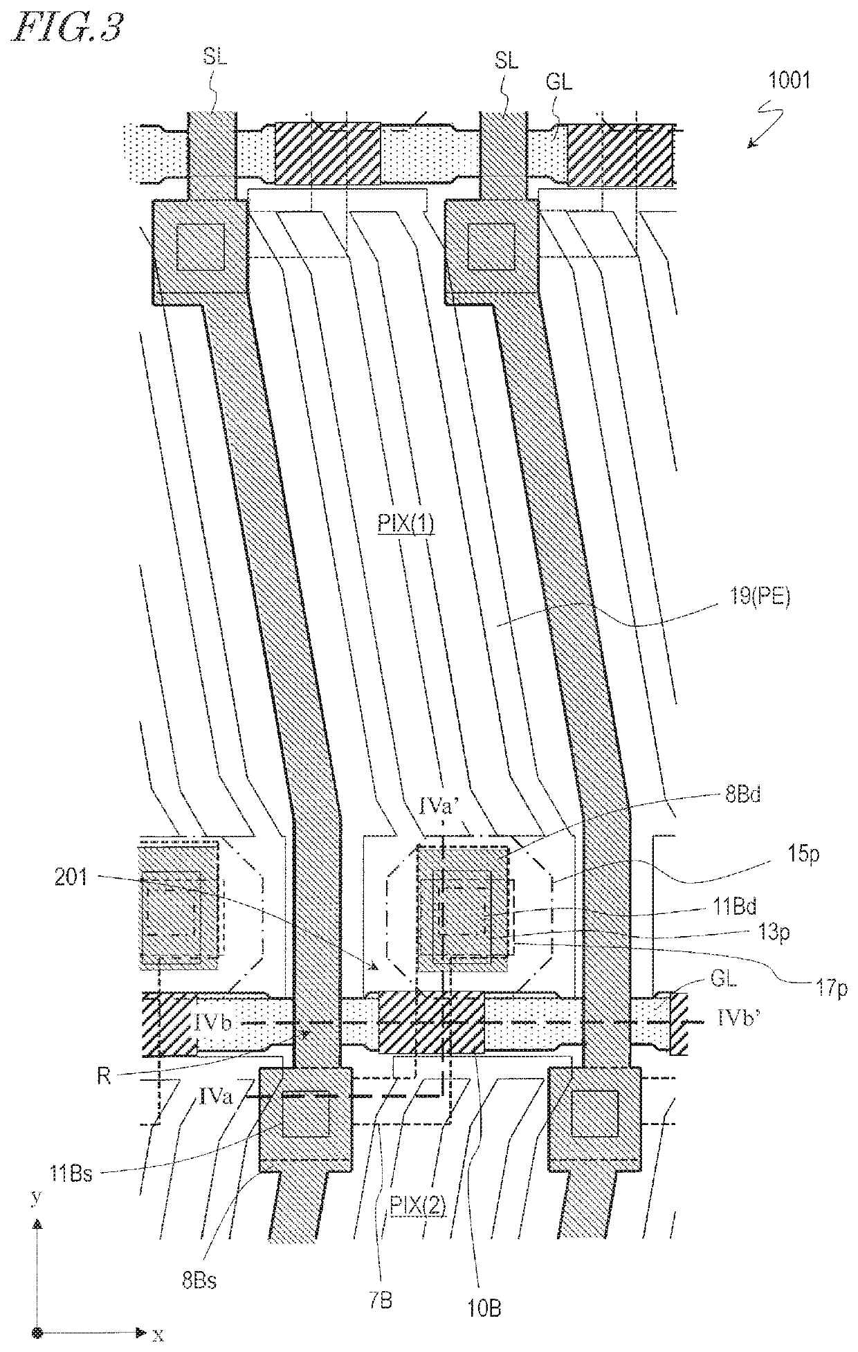
[0187]The present embodiment is different from the first embodiment in that the second TFT (pixel TFT) having the bottom gate structure do not include the island-shaped conductor layer 10B.

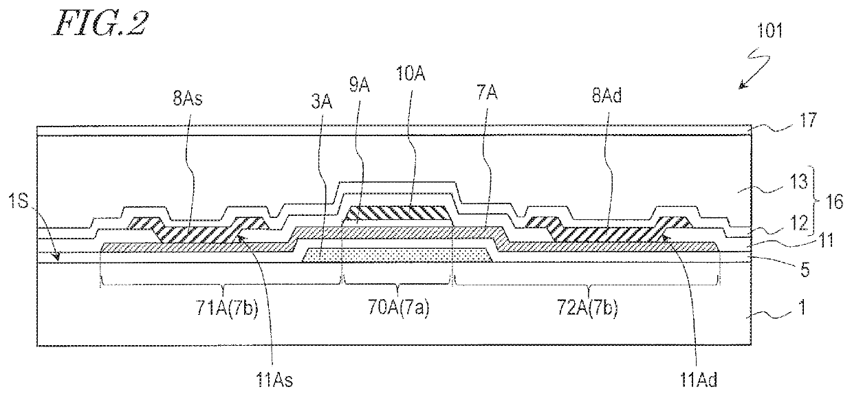
[0188]FIG. 10 is a schematic cross-sectional view showing a first TFT 102, which is a circuit TFT. FIG. 11 is a plan view illustrating a pixel region PIX of an active matrix substrate 1002 of the present embodiment. FIG. 12 is a schematic cross-sectional view of a second TFT 202, which is a pixel TFT, showing a cross-sectional structure taken along line XII-XII′ of FIG. 11. Like elements to those of FIGS. 2 to 4B are denoted by like reference numerals. Like elements to those of the embodiment described above may not be further described below.

[0189]The first TFT 102 is a top gate structure or double gate structure TFT having a similar configuration to that of the ...

third embodiment

[0215]The active matrix substrate of the present embodiment is different from the embodiment described above in that a further insulating layer is arranged in the intersection between the source bus line SL and the gate bus line GL.

[0216]FIG. 15A and FIG. 15B are a plan view and a cross-sectional view taken along line XVb-XVb′, respectively, showing a portion of a pixel region PIX of the present embodiment.

[0217]In the intersection R1 between the source bus line SL and the gate bus line GL, another island-shaped insulator layer (referred to also as the second island-shaped insulator layer) 9R and another island-shaped conductor layer (referred to also as the second island-shaped conductor layer) 10R are arranged between the lower insulating layer 5 and the upper insulating layer 11. The second island-shaped insulator layer 9R is formed by using the same insulating film as the gate insulating layer 9A and the island-shaped insulator layer 9B. The second island-shaped conductor layer ...


PUM


Abstract

An active matrix substrate includes a first TFT of a peripheral circuit and a second TFT arranged in each pixel, wherein: the first TFT is a top gate or double gate TFT that includes an upper gate electrode on a portion of a first oxide semiconductor layer with a gate insulating layer interposed therebetween; the second TFT is a bottom gate TFT that includes a second lower gate electrode arranged on the substrate side of a second oxide semiconductor layer with a lower insulating layer interposed therebetween and includes no gate electrode on the second oxide semiconductor layer; the second TFT including: an island-shaped insulator layer that is arranged on a portion of the second oxide semiconductor layer so as to overlap with at least a portion of the second lower gate electrode, as seen from a direction normal to the substrate; an upper insulating layer that is arranged on the second oxide semiconductor layer and the island-shaped insulator layer; and a source electrode that is arranged on the upper insulating layer, wherein: a portion of the second oxide semiconductor layer that does not overlap with the island-shaped insulator layer is a low resistance region that has a lower specific resistance than a portion thereof that overlaps with the island-shaped insulator layer; and in an intersection between a source bus line and a gate bus line, the lower insulating layer and the upper insulating layer are located between these bus lines.

Description

[0001]This application claims priority to U.S. Provisional Patent Application No. 62 / 733,268 filed on Sep. 19, 2018, the disclosure of which is incorporated herein by reference.BACKGROUND1. Technical Field[0002]The present invention relates to an active matrix substrate using an oxide semiconductor and a method for manufacturing the same.2. Description of the Related Art[0003]Display devices having an active matrix substrate on which a switching element is provided for each pixel have been widely used. An active matrix substrate including thin film transistors (hereinafter “TFTs”) as switching elements is referred to as a TFT substrate. Note that in the present specification, a portion of a TFT substrate that corresponds to a pixel of a display device may also be referred to as a pixel. A TFT provided as a switching element for each pixel of the active matrix substrate is referred to as a “pixel TFT”.[0004]In recent years, it has been proposed to use an oxide semiconductor as the ma...

Claims


Application Information

Patent Timeline
IPC IPC(8): G02F1/1362G02F1/1343G02F1/1333H01L27/32H01L51/56
CPCG02F1/13439H01L51/56H01L27/3258G02F1/136286H01L27/3262G02F1/133345H01L27/3276H01L27/1225H01L27/1251H01L27/124H01L27/1259G02F1/1368H01L29/7869H01L29/78648G02F1/133388H10K59/1213H10K59/1201H01L29/78633H10K59/124H10K59/12H10K59/131H10K59/1315H10K71/00
Inventor MORINAGA, JUNICHIYOSHINO, HIKARU
Owner SHARP KK
Why Eureka
Try Eureka