Electronic module and switching power supply

a technology of switching power supply and electronic module, which is applied in the direction of electric variable regulation, process and machine control, instruments, etc., can solve the problems of complex manufacture of electronic devices, and achieve the effects of reducing noise, reducing manufacturing costs, and increasing the inductance value of inductor

Inactive Publication Date: 2020-03-19
MURATA MFG CO LTD
View PDF0 Cites 2 Cited by
  • Summary
  • Abstract
  • Description
  • Claims
  • Application Information

AI Technical Summary

Benefits of technology

[0011]In an electronic module according to a preferred embodiment of the present invention, at least one of the substrate layers may be a magnetic layer made of a magnetic material, and the fourth connecting conductor may pass through the at least one magnetic layer. This configuration is able to increase the inductance value of the inductor of the snubber circuit. In other words, even if the fourth connecting conductor has a short length, a sufficient inductance value is able to be obtained.
[0019]By using electronic modules according to preferred embodiments of the present invention, electronic devices, such as a switching power supply including a switching element and a snubber circuit, are able to be defined with fewer components. Using the electronic modules also decreases the area of a substrate of an electronic device including a switching element and a snubber circuit. Using the electronic modules also simplifies the manufacturing process of an electronic device including a switching element and a snubber circuit.

Problems solved by technology

In an electronic device, such as a switching power supply, if electronic elements of a snubber circuit are defined by individual electronic components, more components are required in the electronic device, thus making the manufacturing of the electronic device complicated.

Method used


Image

  • Electronic module and switching power supply
  • Electronic module and switching power supply
  • Electronic module and switching power supply

Examples


first preferred embodiment

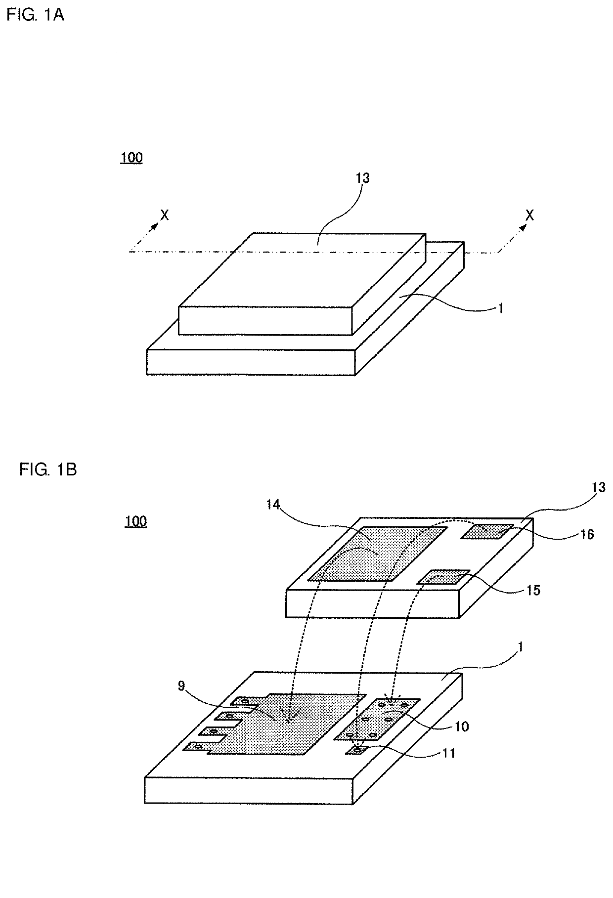
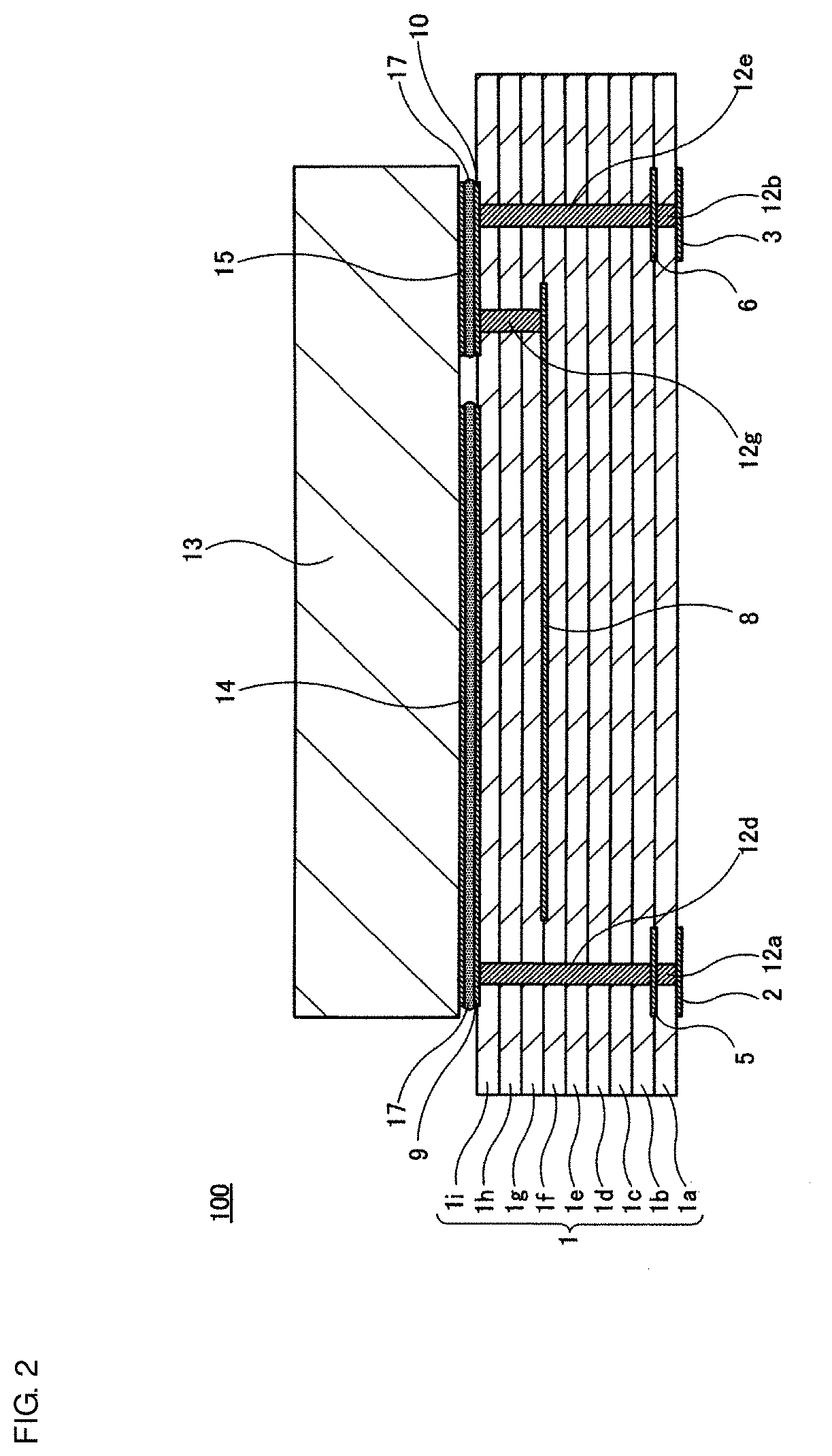
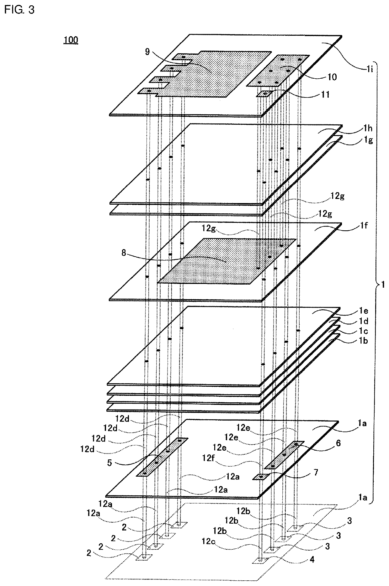
[0037]An electronic module 100 according to a first preferred embodiment of the present invention is shown in FIGS. 1A, 1B, and FIGS. 2, 3, and 4. FIG. 1A is a perspective view of the electronic module 100. FIG. 1B is an exploded perspective view of the electronic module 100 and illustrates the state in which an FET 13 is separated from a multilayer substrate 1 and solder 17 is not shown. FIG. 2 is a sectional view of the electronic module 100 taken along the long dashed dotted line X-X in FIG. 1A. FIG. 3 is an exploded perspective view of the multilayer substrate 1 of the electronic module 100 and illustrates separated nine individual substrate layers 1a through 1i. In FIG. 3, first outer electrodes 2, second outer electrodes 3, and a third outer electrode 4 provided on the lower main surface of the bottommost substrate layer 1a are also indicated by the broken lines. FIG. 4 is an equivalent circuit diagram of the electronic module 100.

[0038]The electronic module 100 includes the m...

second preferred embodiment

[0079]A switching power supply 200 according to a second preferred embodiment of the present invention is shown in FIGS. 5A and 5B. FIG. 5A is a plan view of the switching power supply 200. FIG. 5B is an equivalent circuit diagram of the switching power supply 200.

[0080]The switching power supply 200 is a DC-to-DC converter.

[0081]The switching power supply 200 includes a substrate 25. A preferable material may be used for the substrate 25. The substrate 25 may be a ceramic substrate or a resin substrate, for example. The substrate 25 may be a single-layer substrate or a multilayer substrate. Predetermined outer electrodes, connecting electrodes, and wiring are provided on the substrate 25, though they are not shown.

[0082]On the substrate 25, two electronic modules 100A and 100B, two capacitors C21 and C22, and one inductor L21 are mounted.

[0083]The electronic module 100 of the above-described first preferred embodiment is used for each of the two electronic modules 100A and 100B. A ...

third preferred embodiment

[0088]An electronic module 300 according to a third preferred embodiment of the present invention is shown in FIG. 6. FIG. 6 is an exploded perspective view of the electronic module 300 illustrating the state in which an FET 33 is separated from a multilayer substrate 1.

[0089]The electronic module 300 of the third preferred embodiment is an electronic module obtained by modifying a portion of the configuration of the electronic module 100 of the first preferred embodiment. In the electronic module 100, the drain electrode 14 of the FET 13 is connected to the first connecting electrode 9 of the multilayer substrate 1, the source electrode 15 of the FET 13 is connected to the second connecting electrode 10 of the multilayer substrate 1, and the gate electrode 16 of the FET 13 is connected to the third connecting electrode 11 of the multilayer substrate 1. In the electronic module 300, this configuration is changed. The FET 33 including terminal electrodes arranged differently from tha...


PUM

PropertyMeasurementUnit
electrostatic capacitanceaaaaaaaaaa
areaaaaaaaaaaa
lengthaaaaaaaaaa

Abstract

An electronic module includes a multilayer substrate and an FET. The multilayer substrate includes stacked substrate layers. First and second outer electrodes, a third outer electrode, and first, second, and third connecting electrodes on the multilayer substrate. The first outer electrodes and the first connecting electrode are connected to each other. The second outer electrodes and the second connecting electrode are connected to each other. The third outer electrode and the third connecting electrode are connected to each other. Terminal electrodes of the FET are connected to the first, second, and third connecting electrodes. A second capacitor electrode is between the corresponding layers of the multilayer substrate. A capacitor is defined by electrostatic capacitance between the first connecting electrode and the second capacitor electrode. An inductor is defined by via-conductors connecting the second capacitor electrode and the second connecting electrode. A snubber circuit is defined by the capacitor and the inductor.

Description

CROSS REFERENCE TO RELATED APPLICATIONS[0001]This application claims the benefit of priority to Japanese Patent Application No. 2018-119396 filed on Jun. 23, 2018 and is a Continuation Application of PCT Application No. PCT / JP2019 / 022557 filed on Jun. 6, 2019. The entire contents of each application are hereby incorporated herein by reference.BACKGROUND OF THE INVENTION1. Field of the Invention[0002]The present invention relates to an electronic module in which a switching element is mounted on a multilayer substrate. More particularly, the present invention relates to an electronic module in which a snubber circuit is provided in a multilayer substrate.[0003]The present invention also relates to a switching power supply including the electronic module.2. Description of the Related Art[0004]In some electronic devices, such as switching power supplies, including a switching element, a snubber circuit is disposed to reduce switching noise. For example, Japanese Unexamined Patent Appli...

Claims


Application Information

Patent Timeline
Patent Type & Authority Applications(United States)
IPC IPC(8): H01L23/498H01L23/00H01L23/64H02M3/158H02M1/34
CPCH02M1/34H01L2924/14252H01L2924/19042H01L24/32H01L23/49844H01L2924/19103H02M2001/346H01L23/642H02M3/158H01L2924/19041H01L2224/32227H01L23/645H01L23/49822H01L2924/13091H01L23/49827H01L24/05H01L24/06H01L24/13H01L24/14H01L24/16H01L2224/0603H01L2224/13101H01L2224/1403H01L2224/16225H01L2924/1306H02M1/346H02M3/003Y02B70/10H01L2924/014H01L2924/00014
Inventor KOBAYASHI, NORIFUMI
Owner MURATA MFG CO LTD
Why Eureka
Try Eureka