
Eureka
For R&D, Eureka makes reading and utilizing patents & technical documents easy.
Eureka AIR
Designed for self-driven R&D workflows. Generate viable solutions, solve complex R&D challenges, empower your innovation with AI.

Eureka Materials
Designed for material experts only. Revolutionize your material R&D, from search, analyze, to developing new materials.

TechResearch
Generate reliable direction feasibility study reports for your R&D in just a few steps.

TechSeek
Discover and master advanced knowledge NOW. Basics, ideas, possibilities, all at once.

TechMind
As an expert in R&D Theories, TechMind can generates customized viable solutions instantly.

TechRisk
Analyze your overall solution with one click, know your potential R&D risks in advance.

TechMonitor
Get weekly tech updates, stay abreast of the latest tech innovations and key insights.
Just in time data placement in NAND flash
- Summary
- Abstract
- Description
- Claims
- Application Information
AI Technical Summary
Benefits of technology
Problems solved by technology
Method used
Image

Examples
Embodiment Construction
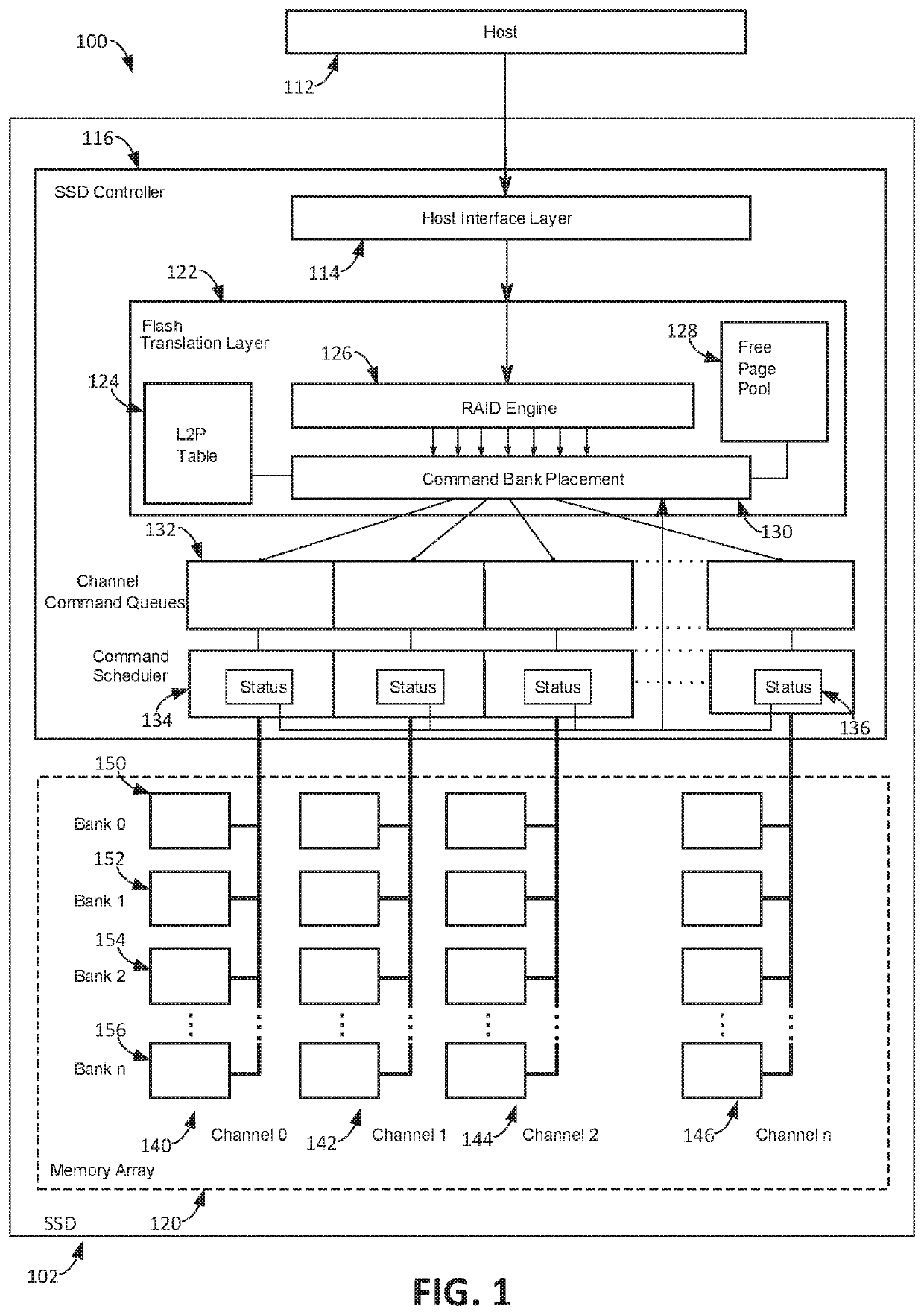
[0019]FIG. 1 is a system diagram 100 schematically illustrating the structure of a solid-state drive (SSD) 102, in accordance with an embodiment of the present invention.
[0020]The host device 112 connects to the SSD 102 via a host interface layer 114 conforming to a communication interface standard. The SSD 102 functions as an external mass storage device of the host device 112. Examples of the communication interface standard between the SSD 102 and the host device 112 include SATA (Serial Advanced Technology Attachment), SAS (Serial Attached SCSI), PCIe (Peripheral Components Interconnect Express).
[0021]The SSD 102 comprises a SSD controller 116 and a memory array 120, which in an embodiment comprises an array of NAND devices. The SSD controller 116 comprises a host interface layer 114 and a flash translation layer (FTL) 122. The FTL 122 includes a logic-to-physical (L2P) table 124, a RAID engine 126, a free page pool 128, and a command bank placement function 130. The command ban...
PUM
 Abstract
Description
Claims
Application Information
 - R&D Engineer
- R&D Manager
- IP Professional
- Industry Leading Data Capabilities
- Powerful AI technology
- Patent DNA Extraction
Browse by: Latest US Patents, China's latest patents, Technical Efficacy Thesaurus, Application Domain, Technology Topic, Popular Technical Reports.
© 2024 PatSnap. All rights reserved.Legal|Privacy policy|Modern Slavery Act Transparency Statement|Sitemap|About US| Contact US: help@patsnap.com