Integrated circuit structure with complementary field effect transistor and buried metal interconnect and method

a technology of integrated circuits and transistors, applied in the field of complementary field effect transistors, can solve the problems of quite complex signal connection to the source/drain region of the lower-level gaafets (e.g., )

Active Publication Date: 2020-04-09
GLOBALFOUNDRIES US INC
View PDF3 Cites 20 Cited by
  • Summary
  • Abstract
  • Description
  • Claims
  • Application Information

AI Technical Summary

Problems solved by technology

While using CFETs can increase on-chip device density and reduce area consumption, providing signal connections to the source / drain regions of the lower-level GAAFETs (e.g., to achieve the cross-couple connection in an SRAM cell) can be quite complex.

Method used


Image

  • Integrated circuit structure with complementary field effect transistor and buried metal interconnect and method
  • Integrated circuit structure with complementary field effect transistor and buried metal interconnect and method
  • Integrated circuit structure with complementary field effect transistor and buried metal interconnect and method

Examples


Embodiment Construction

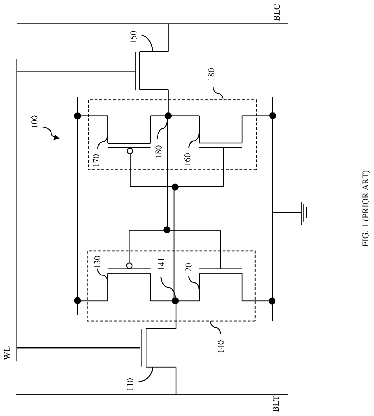
[0036]As mentioned above, a complementary field effect transistor (CFET) typically includes an N-type gate-all-around field effect transistor (GAAFET) on one-level, a P-type GAAFET on an adjacent level (i.e., above or below) and, a common gate that extends vertically across and wraps around the stacked channel regions of the N-type and P-type GAAFETs. Typically, the source / drain regions of the lower-level GAAFET will be electrically isolated from the source / drain regions of the upper-level GAAFET by one or more isolation layers. Such CFETs can, for example, be incorporated into a six-transistor (6T) static random access memory (SRAM) cell, one for each pair of pull-down and pull-up field effect transistors, respectively. While using CFETs can increase on-chip device density and reduce area consumption, providing signal connections to the source / drain regions of the lower-level GAAFETs (e.g., to achieve the cross-couple connection in an SRAM cell) can be quite complex.

[0037]For examp...


PUM

PropertyMeasurementUnit
work functionaaaaaaaaaa

Abstract

Disclosed are structures with a complementary field effect transistor (CFET) and a buried metal interconnect that electrically connects a source / drain region of a lower-level transistor of the CFET with another device. The structure can include a memory cell with first and second CFETs, where each CFET includes a pull-up transistor stacked on and having a common gate with a pull-down transistor and each pull-down transistor has a common source / drain region with a pass-gate transistor. The metal interconnect connects a lower-level source / drain region of the first CFET (i.e., the common source / drain region of first pass-gate and pull-up transistors) to the common gate of the second CFET (i.e., to the common gate of second pull-down and pull-up transistors). Formation methods include forming an interconnect placeholder during lower-level source / drain region formation. After upper-level source / drain regions and replacement metal gates are formed, the interconnect placeholder is exposed, removed and replaced with a metal interconnect.

Description

BACKGROUNDField of the Invention[0001]The present invention relates to complementary field effect transistors (CFETs) and, more particularly, to an integrated circuit (IC) structure with a CFET and a buried metal interconnect that enables an electrical connection to a source / drain region of a lower-level transistor within the CFET and to a method of forming the IC structure.Description of Related Art[0002]Gate-all-around field effect transistors (GAAFETs) (e.g., nanowire-type GAAFETs or nanosheet-type GAAFETs) have been developed in order to improve drive current and electrostatics and to allow for device size scaling, increased device density and reduced area consumption. A GAAFET includes elongated nanoshape(s) (e.g., nanowire(s) or nanosheet(s)), which extend laterally between source / drain regions, and a wrap-around gate structure, which wraps around the nanoshape(s) such that the nanoshape(s) function as channel region(s).[0003]Recently, complementary field effect transistors (C...

Claims


Application Information

Patent Timeline
Patent Type & Authority Applications(United States)
IPC IPC(8): H01L27/11H01L23/528H01L21/768
CPCH01L21/76883H01L21/76816H01L29/7853H01L21/76843H01L29/0673H01L29/42392H01L27/1108H01L21/76805H01L23/5283H01L29/78696H01L27/0207H01L27/092H01L29/66439H01L29/41733H01L27/124H01L29/66772H01L29/78654H01L29/66545H01L27/0688H01L21/8221H01L21/823871H01L21/823814H01L21/76895H01L21/76897H01L29/775B82Y10/00H01L21/743H01L23/535H10B10/125
Inventor PAUL, BIPUL C.XIE, RUILONG
Owner GLOBALFOUNDRIES US INC
Why Eureka
Try Eureka