Finfet structure with dielectric bar containing gate to reduce effective capacitance, and method of forming same

a dielectric bar and gate technology, applied in the direction of transistors, electrical apparatus, semiconductor devices, etc., can solve the problem of complicating the parasitic capacitance of finfet devices, and achieve the effect of reducing effective capacitan

Active Publication Date: 2020-04-30
GLOBALFOUNDRIES US INC
View PDF12 Cites 1 Cited by
  • Summary
  • Abstract
  • Description
  • Claims
  • Application Information

AI Technical Summary

Benefits of technology

[0003]FinFET structures containing a dielectric bar within the gate area and having reduced effective capacitance and methods of forming the same are disclosed. In a first aspect of the disclosure, a FinFET structure includes: a substrate having at least two fins thereon laterally spaced from one another; a metal gate over fin tops of the at least two fins and between sidewalls of upper portions of the at least two fins; source / drain regions in each fin on opposing sides of the metal gate; and a dielectric bar within the metal gate located between the sidewalls of the upper portions of the at least two fins, the dielectric bar being laterally spaced away from the sidewalls of the upper portions of the at least two fins within the metal gate.

Problems solved by technology

But, it also complicates the parasitic capacitance of the FinFET device.

Method used


Image

  • Finfet structure with dielectric bar containing gate to reduce effective capacitance, and method of forming same
  • Finfet structure with dielectric bar containing gate to reduce effective capacitance, and method of forming same
  • Finfet structure with dielectric bar containing gate to reduce effective capacitance, and method of forming same

Examples


Embodiment Construction

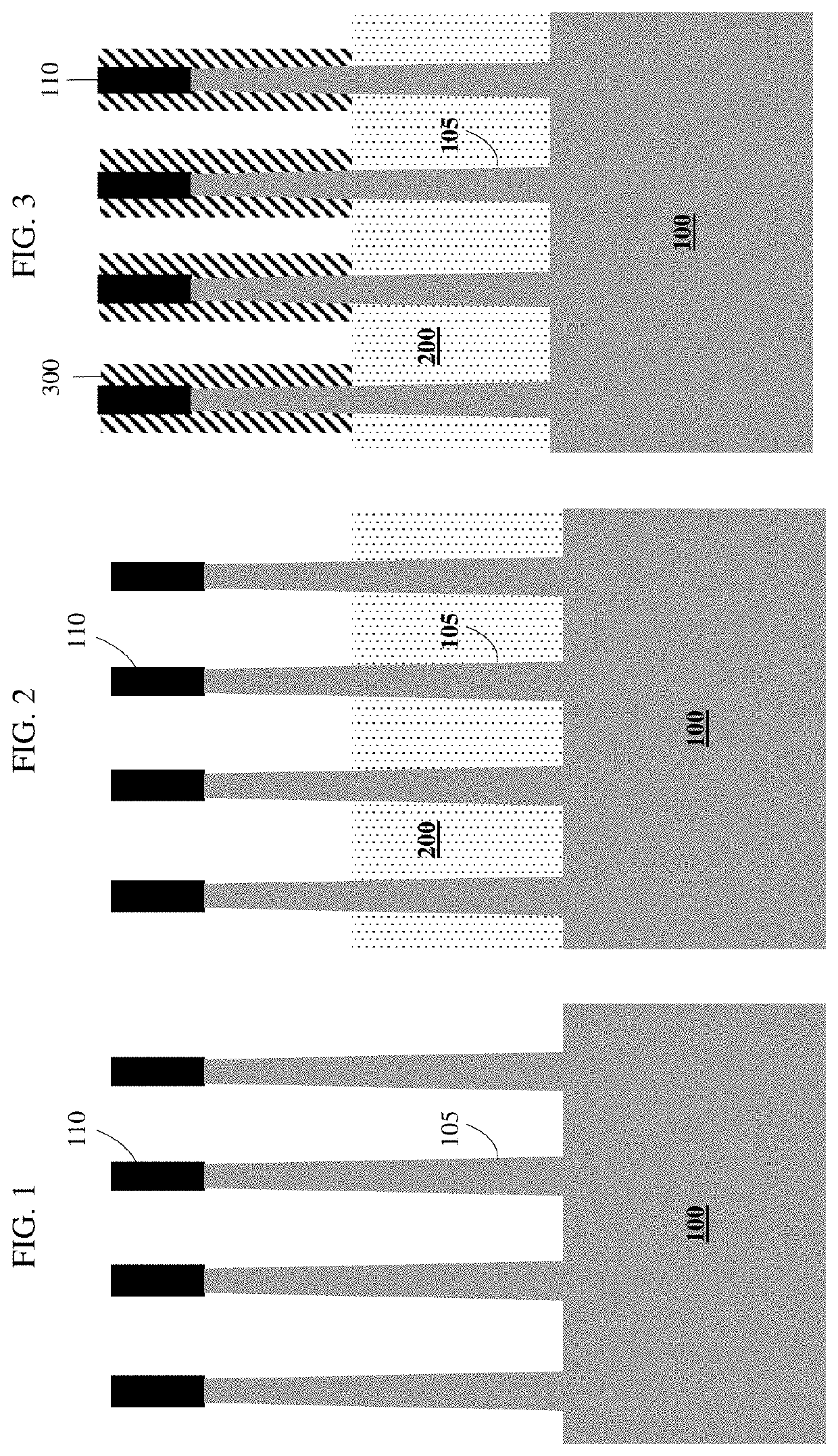
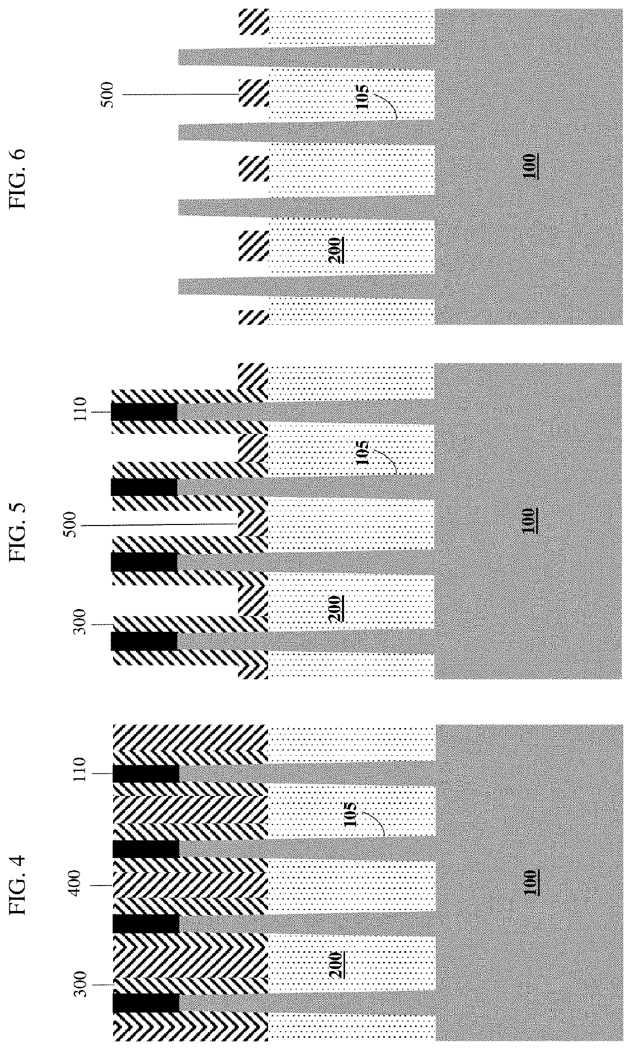
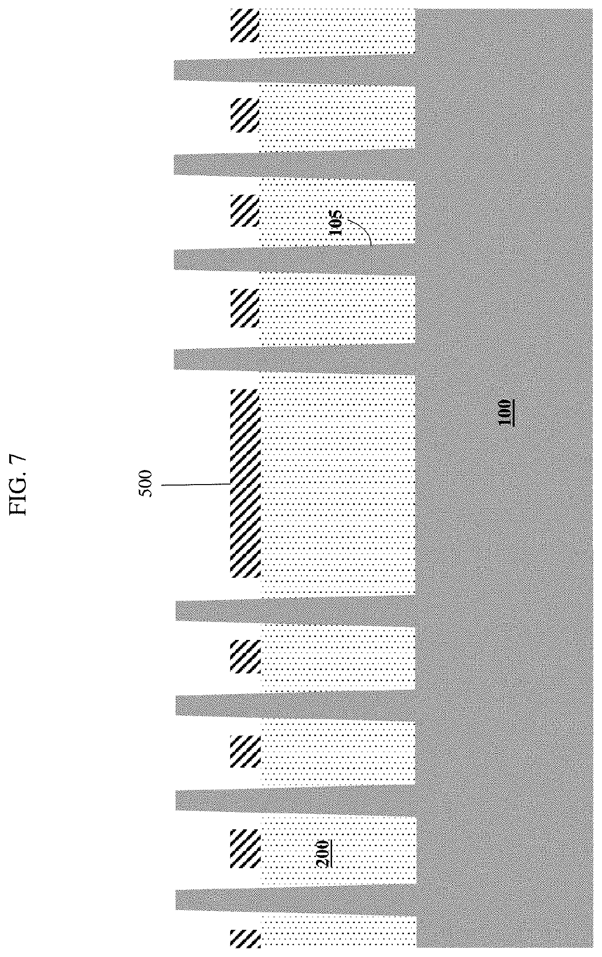
[0017]The subject matter disclosed herein relates to FinFET structures containing a dielectric bar within the gate area. More specifically, various aspects described herein relate to FinFET structures containing a dielectric bar within the gate area and having reduced effective capacitance, and methods of forming the same.

[0018]As noted above, conventional scaled down FinFETs (such as 14 nm and beyond) can suffer from excessive gate-to-contact parasitic capacitance which can significantly increase an integrated circuit's (IC) effective capacitance (Ceff) and thus degrade chip performance. In contrast, various aspects of the disclosure include FinFET structures containing one or more dielectric bars within the gate area that allow for reduced gate-to-contact parasitic capacitance which in turn allows for reduced effective capacitance of an IC and improved device performance.

[0019]FIG. 1 depicts a starting precursor FinFET structure that may be formed by any now known or later develop...


PUM

PropertyMeasurementUnit
distanceaaaaaaaaaa
distanceaaaaaaaaaa
thicknessaaaaaaaaaa

Abstract

A FinFET structure having reduced effective capacitance and including a substrate having at least two fins thereon laterally spaced from one another, a metal gate over fin tops of the fins and between sidewalls of upper portions of the fins, source/drain regions in each fin on opposing sides of the metal gate, and a dielectric bar within the metal gate located between the sidewalls of the upper portions of the fins, the dielectric bar being laterally spaced away from the sidewalls of the upper portions of the fins within the metal gate.

Description

TECHNICAL FIELD[0001]The subject matter disclosed herein relates to FinFET structures containing a dielectric bar within the gate area. More specifically, various aspects described herein relate to FinFET structures containing a dielectric bar within the gate area and having reduced effective capacitance, and methods of forming the same.BACKGROUND[0002]With complementary metal-oxide semiconductor (CMOS) technology continuously scaling down, the three-dimensional (3-D) fin field-effect transistor (FinFET) device has become the mainstream device due to its better electrostatic control and reduced junction capacitance. The 3-D structure provides a new electric field distribution in the channel and improves the current-voltage characteristic curves. But, it also complicates the parasitic capacitance of the FinFET device. More specifically, as FinFET devices scale down, the gate-to-contact parasitic capacitance gradually dominates the total capacitance of the device.BRIEF SUMMARY[0003]Fi...

Claims


Application Information

Patent Timeline
Patent Type & Authority Applications(United States)
IPC IPC(8): H01L27/088H01L29/08H01L29/66H01L29/51H01L29/78H01L29/49H01L21/8234
CPCH01L21/823481H01L29/66545H01L29/785H01L29/0847H01L21/823431H01L21/823468H01L27/0886H01L29/51H01L29/4966H01L21/823437
Inventor ZANG, HUIWANG, HAITINGTAN, CHUNG FOONGXU, GUOWEIXIE, RUILONGBEASOR, SCOTT H.JIANG, LIU
Owner GLOBALFOUNDRIES US INC
Why Eureka
Try Eureka