Supercharge Your Innovation With Domain-Expert AI Agents!

Method of manufacturing semiconductor devices

a technology of semiconductor chips and manufacturing methods, applied in the direction of sustainable manufacturing/processing, final product manufacturing, non-macromolecular adhesive additives, etc., can solve the problems of deterioration of the reliability of the semiconductor package, and achieve the effect of improving the reliability of the semiconductor device/packag

Active Publication Date: 2020-05-07
SAMSUNG ELECTRONICS CO LTD
View PDF0 Cites 0 Cited by
  • Summary
  • Abstract
  • Description
  • Claims
  • Application Information

AI Technical Summary

Benefits of technology

This patent presents a method for making a semiconductor device / package more reliable. The method involves creating a cured film that fills the gap between the chip and substrate, preventing any empty spaces. The film is also minimized to avoid overflow. This results in a package that is more reliable and secure.

Problems solved by technology

The adhesive material may be cured by a thermo-compression process to form a cured film, however, the cured film may not entirely cover the semiconductor chip or may protrude from the semiconductor chip by the thermos-compression process, and in this case, the reliability of the semiconductor package may be deteriorated.

Method used


Image

  • Method of manufacturing semiconductor devices
  • Method of manufacturing semiconductor devices
  • Method of manufacturing semiconductor devices

Examples


Embodiment Construction

[0014]An adhesion method of semiconductor chips in accordance with example embodiments will be described more fully hereinafter with reference to the accompanying drawings.

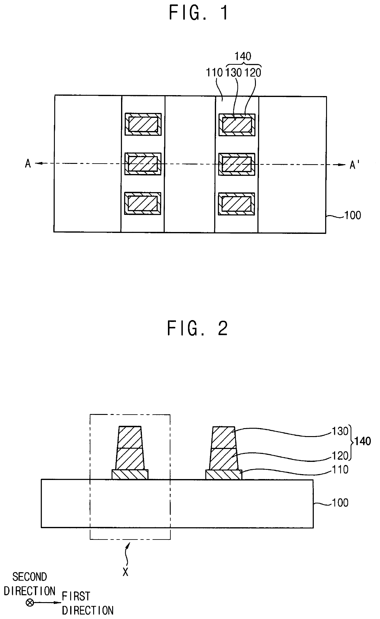
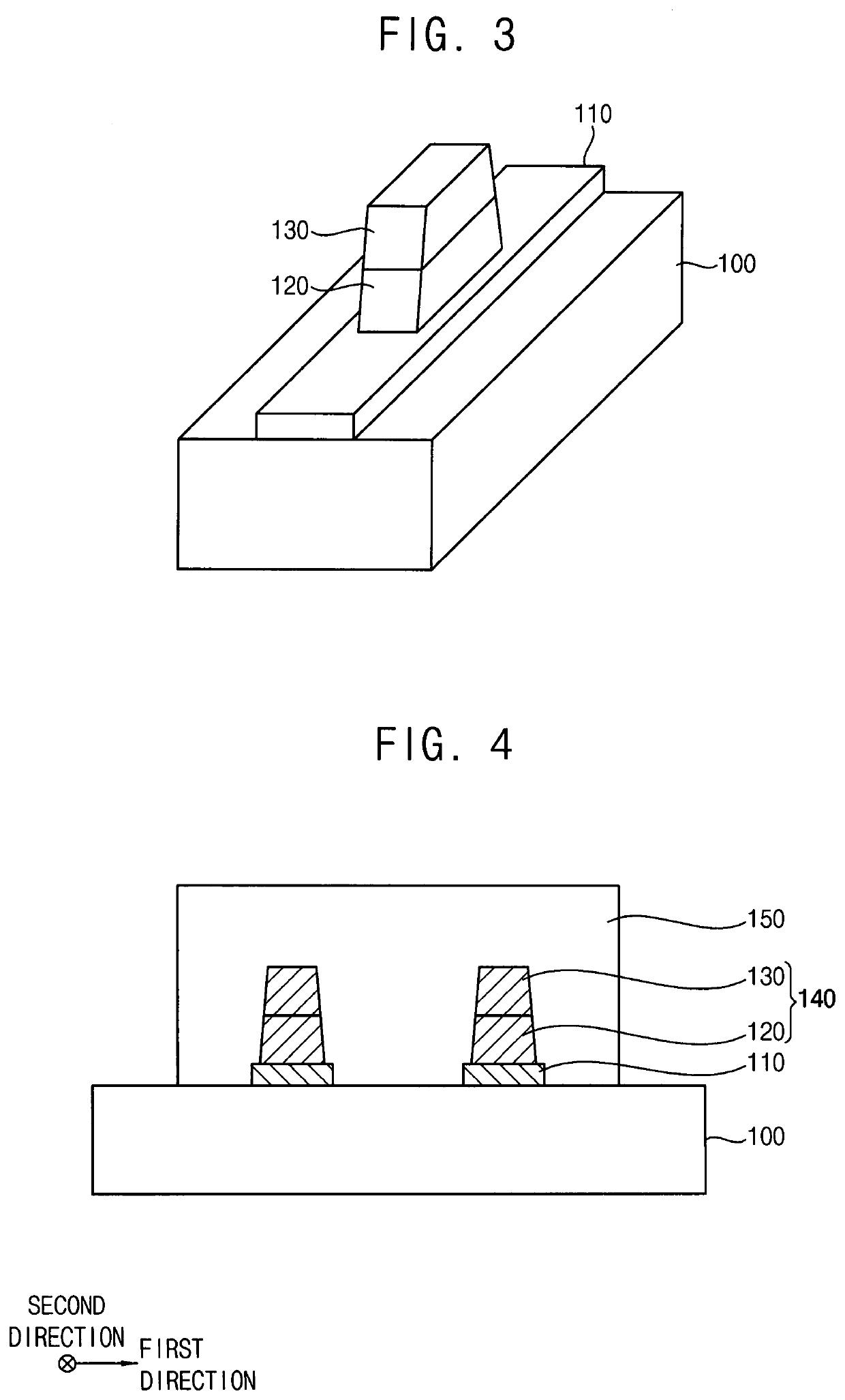
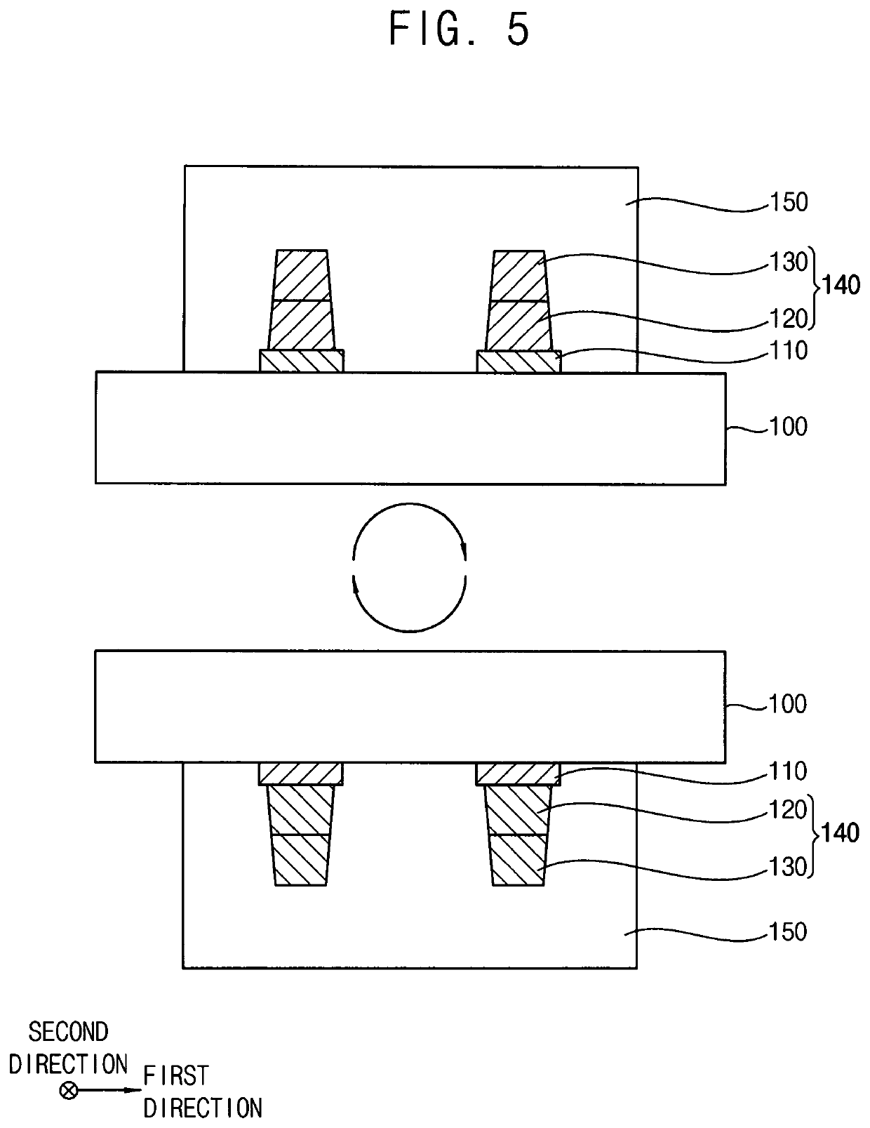
[0015]FIGS. 1 to 11 are respectively plan views, cross-sectional views and a perspective view illustrating an adhesion method of semiconductor chips in accordance with example embodiments. Specifically, FIGS. 1, 7-8 and 10-11 are the plan views, FIGS. 2, 4-6 and 9 are cross-sectional views taken along lines A-A′ of corresponding plan views, respectively, and FIG. 3 is an enlarged perspective view of a region X of FIG. 2.

[0016]Referring to FIGS. 1 to 3, a conductive bump structure 140 including a first conductive bump 120 and a second conductive bump 130 sequentially stacked may be formed on a semiconductor chip 100 including a chip pad 110. For example, the first conductive bump 120 and the second conductive bump 130 may be sequentially stacked on the chip pad 110.

[0017]For example, after forming a seed layer (not...


PUM

PropertyMeasurementUnit
Temperatureaaaaaaaaaa
Forceaaaaaaaaaa
Angleaaaaaaaaaa

Abstract

A method of manufacturing a semiconductor device may include forming an adhesive film on a surface of a semiconductor chip, mounting the semiconductor chip on a substrate such that the adhesive film contacts an upper surface of the substrate, and bonding the semiconductor chip and the substrate curing the adhesive film by simultaneously performing a thermo-compression process and an ultraviolet irradiation process on the adhesive film disposed between the substrate and the semiconductor chip.

Description

CROSS-REFERENCE TO RELATED APPLICATION[0001]This application claims priority under 35 USC § 119 to Korean Patent Application No. 10-2018-0135345, filed on Nov. 6, 2018 in the Korean Intellectual Property Office (KIPO), the contents of which are herein incorporated by reference in their entirety.BACKGROUND1. Field[0002]Example embodiments relate to an adhesion method of semiconductor chips. More particularly, example embodiments relate to an adhesion method of semiconductor chips using an adhesive material.2. Description of the Related Art[0003]In a method of manufacturing a semiconductor package, an adhesive material may be used for bonding a semiconductor chip and a substrate. The adhesive material may be in a form of a non-conductive paste (NCP) or a non-conductive film (NCF) including a thermosetting resin.[0004]The adhesive material may be cured by a thermo-compression process to form a cured film, however, the cured film may not entirely cover the semiconductor chip or may prot...

Claims


Application Information

Patent Timeline
IPC IPC(8): H01L23/00H05K3/32C09J5/06H01L21/50
CPCH05K3/323H01L24/95H01L2021/603H01L2021/60277C09J5/06H01L21/50H01L24/83H01L24/29H01L2224/83026H01L2224/83203H01L2224/8322H01L2224/83488H01L21/563C09J2203/326C09J2301/416C09J2433/00H05K3/305H01L2224/05568H01L2224/0401H01L2224/13082H01L2224/13013H01L2224/13014H01L2224/81191H01L2224/83191H01L2224/73104H01L2224/75261H01L2224/83874H01L2224/83862H01L2224/831H01L2224/75251H01L2224/75252H01L2224/75253H01L2224/83859H01L2224/83885H01L2224/32225H01L2224/16238H01L2224/32058H01L2224/83192H01L2224/27436H01L2224/2731H01L2224/73204H01L24/32H01L2224/14151H01L2224/13109H01L2224/2939H01L2224/29355H01L2224/13111H01L2224/29324H01L2224/29339H01L2224/2929H01L2224/29386H01L2224/05638H01L2224/81399H01L2224/13139H01L2224/13155H01L2224/13147H01L2224/2919Y02P70/50H01L2224/16145H01L2224/32145H01L2924/00014H01L2224/16225H01L2924/00H01L2924/0665H01L2924/05032H01L2924/013H01L2924/0105H01L2924/01014H01L2924/05432H01L2924/05442H01L2924/07001H01L2924/0635H01L2924/05341H01L2924/01029H01L2924/01047H01L2924/01049H01L2924/0685H01L2924/0503H01L2924/01005H01L2924/05042H01L21/52H01L21/67092H01L21/67098H01L21/67248H01L24/27H01L24/11C09J163/00C09J133/00C09J183/04C09J11/06C09J11/04H01L21/603
Inventor KIM, YEONG-SEOK
Owner SAMSUNG ELECTRONICS CO LTD
Features
  • R&D
  • Intellectual Property
  • Life Sciences
  • Materials
  • Tech Scout
  • Unparalleled Data Quality
  • Higher Quality Content
  • 60% Fewer Hallucinations
Learn More