System and method of duplicate circuit block swapping for noise reduction

a technology of circuit block swapping and noise reduction, applied in the direction of oscillator generator, amplifier modification to reduce noise influence, etc., can solve the problems of audio circuits, circuits and applications that operate with relatively long time constants, require relatively high accuracy, improper operation or erroneous operation, etc., and achieve the effect of reducing noise on a semiconductor circui

Active Publication Date: 2020-06-18
SILICON LAB INC
View PDF0 Cites 1 Cited by
  • Summary
  • Abstract
  • Description
  • Claims
  • Application Information

AI Technical Summary

Benefits of technology

[0011]A method of reducing noise on a semiconductor circuit according to one embodiment includes providing at least one circuit node on the semiconductor circuit, integrating multiple duplicate circuit blocks on the semiconductor circuit in close proximity with each other, each including at least one device that is susceptible to random telegraph noise (RTN), and swapping electrical coupling of the duplicate circuit blocks, one at a time, to the at least one circuit node in sequential cycles of a clock signal.

Problems solved by technology

The characteristics of RTN present a challenge for circuits and applications that operate with relatively long time constants and that require relatively high accuracy.
Clock circuits used for keeping time, for example, may suffer from RTN causing improper operation or erroneous results.
Audio circuits may also suffer from RTN causing spurious or unwanted audible noise.
Semiconductor parts that operate with a relatively large time constant and that fail specifications due to RTN are very difficult to screen at production test since the testing time necessary to detect failure is prohibitively long.
Thus, it is not cost effective to screen parts during production test.

Method used


Image

  • System and method of duplicate circuit block swapping for noise reduction
  • System and method of duplicate circuit block swapping for noise reduction
  • System and method of duplicate circuit block swapping for noise reduction

Examples


Embodiment Construction

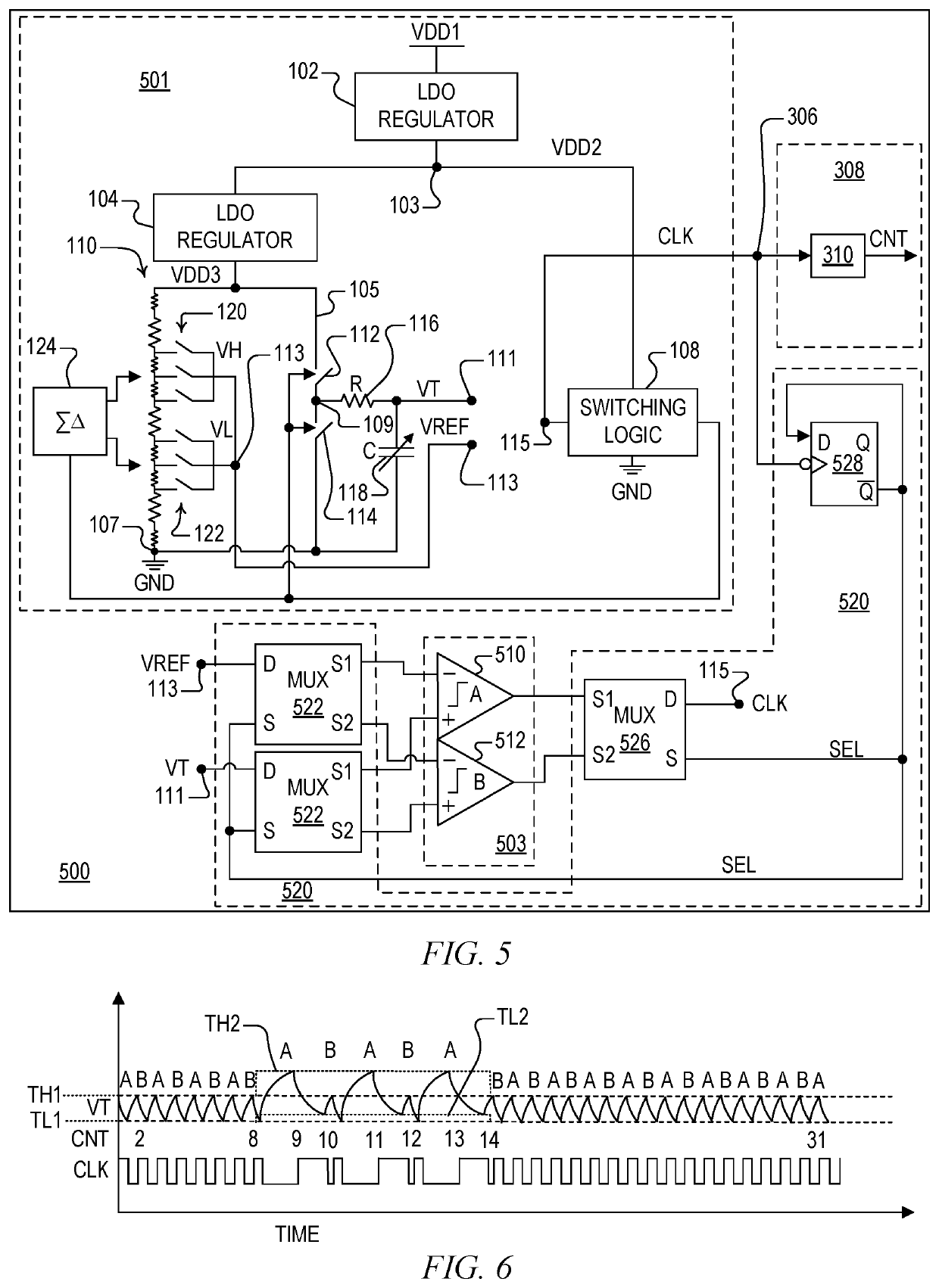
[0030]The inventors have recognized the problems associated with RTN and also the difficulty in detecting RTN during production testing. They have therefore developed a system and method of duplicate circuit block swapping to reduce RTN. RTN is reduced without the need to identify the source of RTN causing the performance degradation. Although large functional circuits may be duplicated and swapped out during operation to reduce noise and improve operation, judicious selection of the duplicated circuit block may reduce the area and power penalty associated therewith.

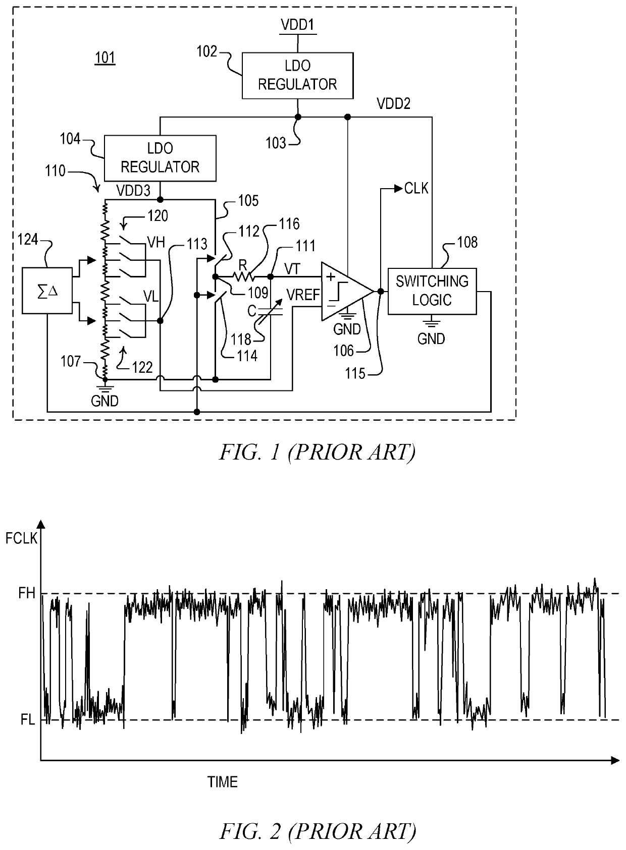
[0031]FIG. 1 is a schematic and block diagram of a conventional relaxation oscillator 101, such as described in U.S. Pat. No. 9,823,687, entitled “LOW FREQUENCY PRECISION OSCILLATOR,” issued Nov. 13, 2017 to Mukherji et al. A first low dropout (LDO) regulator 102 receives a first supply voltage VDD1 and provides a second supply voltage VDD2 on a supply node 103, and a second LDO regulator 104 receives VDD2 and provides a...


PUM


Abstract

An integrated circuit including at least one circuit node, multiple duplicate circuit blocks integrated on the integrated circuit in close proximity with each other, each including at least one device that is susceptible to random telegraph noise (RTN), and a switch circuit that swaps electrical coupling of the duplicate circuit blocks, one at a time, to the at least one circuit node in sequential cycles of a clock signal. The duplicate circuit blocks may be large functional blocks, such as an oscillator or a comparator or the like, or limited to circuits including RTN susceptible devices, such as differential pairs or the like. Each duplicate circuit block may include any number of connections for coupling to corresponding circuit nodes. The swapping may further include chopping in which multiple inputs are swapped with each other while multiple outputs are swapped with each other in consecutive clock cycles.

Description

BACKGROUND OF THE INVENTIONField of the Invention[0001]The present invention relates in general to electronic circuit noise reduction, and more particularly to a system and method of sequentially replacing or swapping duplicate circuit blocks to reduce Random Telegraph Noise (RTN) or “popcorn” noise in an electronic circuit.Description of the Related Art[0002]Random Telegraph Noise (RTN) or “popcorn” noise is characterized by sudden voltage or current transitions between two or more discrete levels in semiconductor devices. The characteristics of RTN present a challenge for circuits and applications that operate with relatively long time constants and that require relatively high accuracy. Clock circuits used for keeping time, for example, may suffer from RTN causing improper operation or erroneous results. Audio circuits may also suffer from RTN causing spurious or unwanted audible noise. Semiconductor parts that operate with a relatively large time constant and that fail specifica...

Claims


Application Information

Patent Timeline
Patent Type & Authority Applications(United States)
IPC IPC(8): G01R29/26G06F1/04H03B5/20
CPCG06F1/04H03B5/20G01R29/26H03F1/26H03K5/1252
Inventor PEREIRA, VITORMUKHERJI, ARUP
Owner SILICON LAB INC
Why Eureka
Try Eureka