Semiconductor device
- Summary
- Abstract
- Description
- Claims
- Application Information
AI Technical Summary
Benefits of technology
Problems solved by technology
Method used
Image

Examples
Embodiment Construction
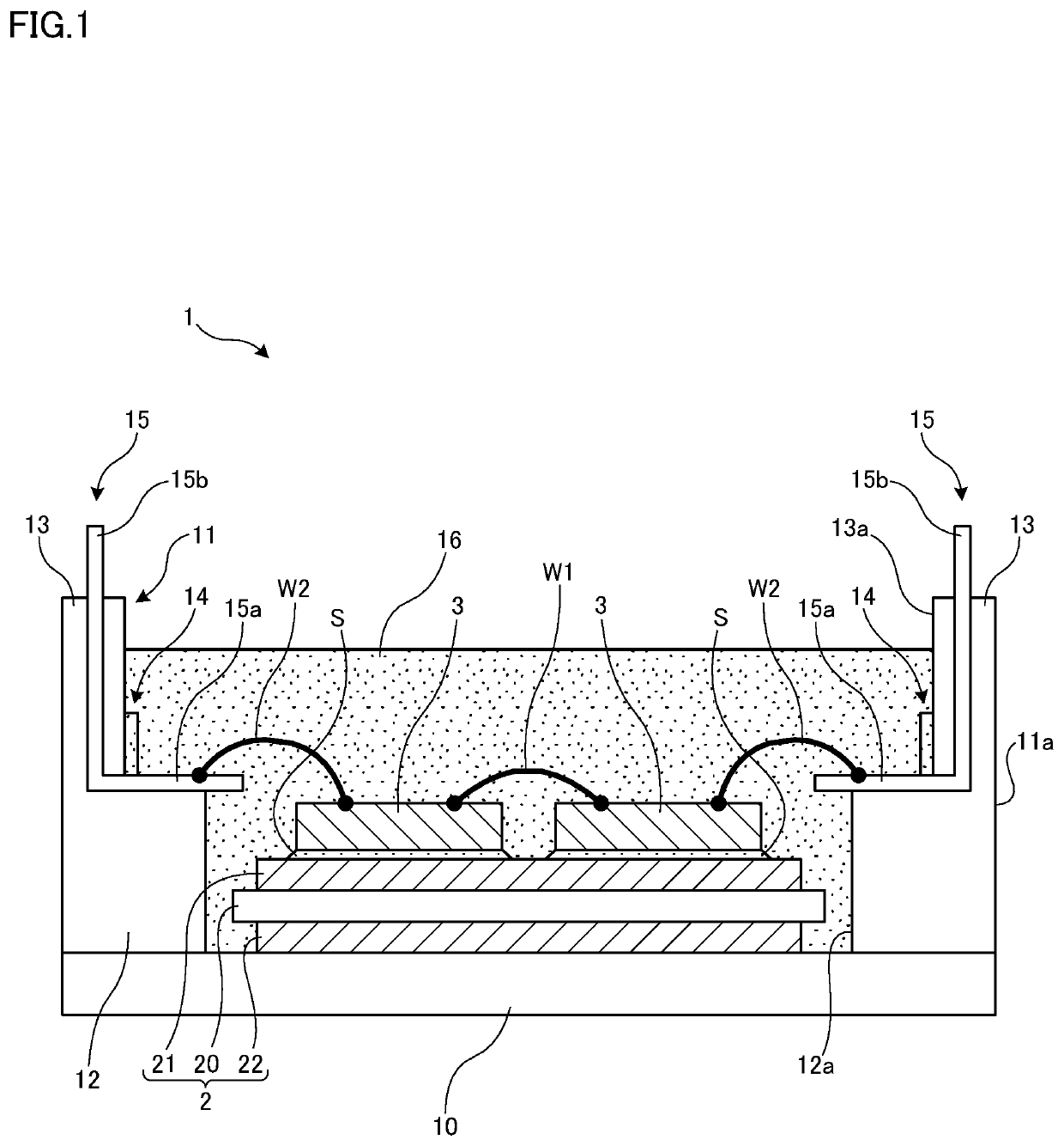
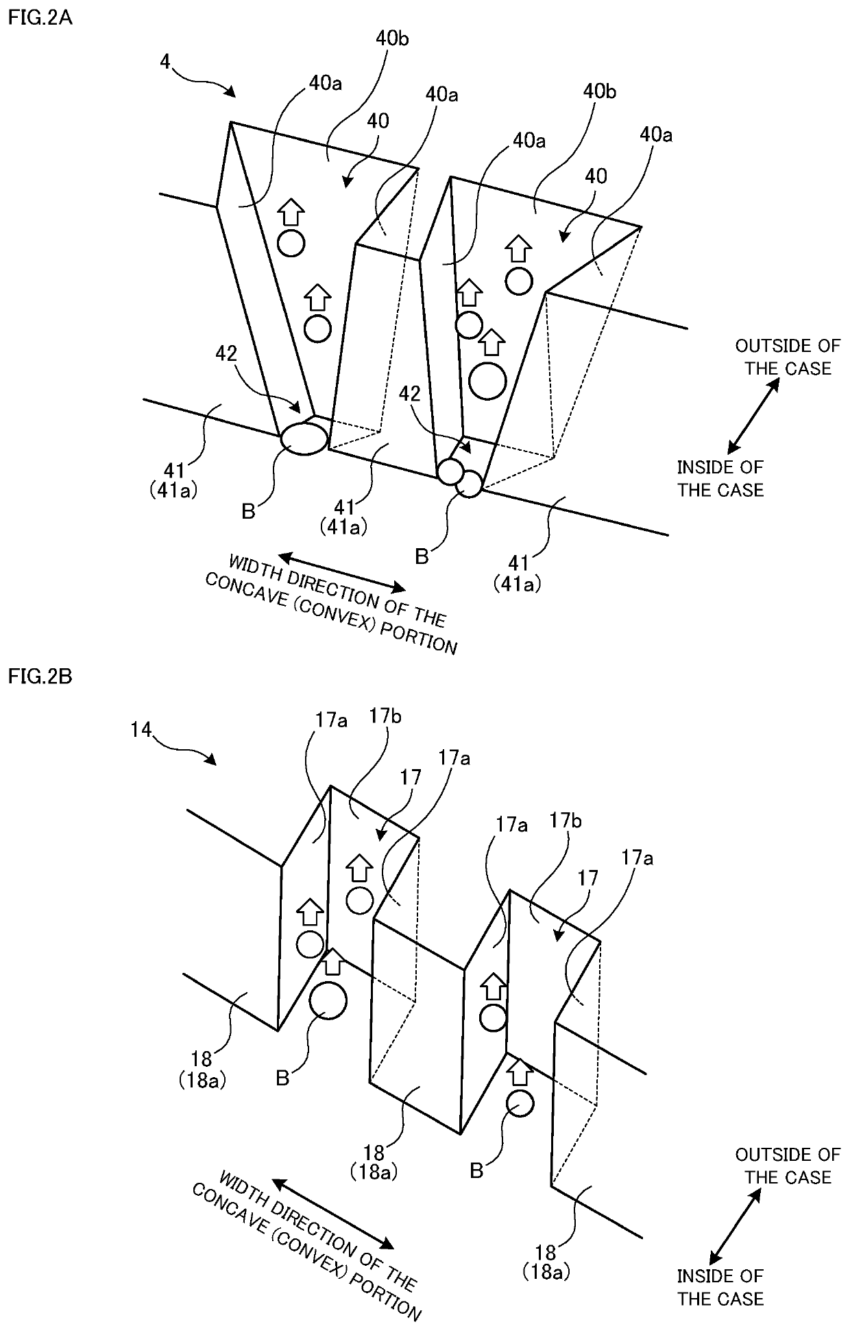
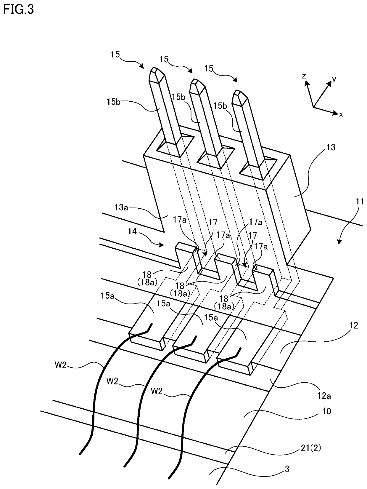
[0018]Hereinafter, a semiconductor device to which the present invention can be applied will be described. FIG. 1 is a schematic cross-sectional view illustrating an exemplary semiconductor device according to the present embodiment. Note that the semiconductor device described below is merely an example, and the present invention is not limited to this and can be changed appropriately.
[0019]A semiconductor device 1 is, for example, applied to a power conversion device such as a power module. As illustrated in FIG. 1, the semiconductor device 1 includes an insulated circuit board 2, and semiconductor elements 3 disposed on an upper surface of the insulated circuit board 2. The semiconductor device 1 further includes a case 11 that surrounds the insulated circuit board 2 and the semiconductor elements 3. Further, the semiconductor device 1 may include a base plate 10. For example, the base plate 10 has a rectangular shape in plan view, and is formed of a metal (e.g., copper) plate. T...
PUM
 Abstract
Description
Claims
Application Information
 - R&D Engineer
- R&D Manager
- IP Professional
- Industry Leading Data Capabilities
- Powerful AI technology
- Patent DNA Extraction
Browse by: Latest US Patents, China's latest patents, Technical Efficacy Thesaurus, Application Domain, Technology Topic.
© 2024 PatSnap. All rights reserved.Legal|Privacy policy|Modern Slavery Act Transparency Statement|Sitemap