Light emitting diode and manufacturing method thereof

Active Publication Date: 2020-07-09
GENESIS PHOTONICS
View PDF0 Cites 0 Cited by
  • Summary
  • Abstract
  • Description
  • Claims
  • Application Information

AI Technical Summary

Benefits of technology

[0021]To sum up, in the LED provided by the embodiments of the invention, the contact scope of the current conducting layer and the second-type semiconductor layer is served as the light-emitting scope, and the first and the second reflective layers overlap the light-emitting scope. Additionally, the main light emitting surface is formed on one of the first and the second reflective layers, and the light transmittance of the main light emitting surface is greater than 0% and less than or equal to 10%. Thus, a part of light beams emitted from the active layer are transmitted through the first reflective layer (or the second reflective layer), and a part of the light beams are reflected between the first

Problems solved by technology

As an optical fiber has a small light-receiving area, the optic fiber is incapable of effectively receiving the light if a light-emitting angle of a light source is too large, and thus, a light source capable of emitting a high directional light is required to serve as a light source of an optic fiber communication transceive

Method used


Image

  • Light emitting diode and manufacturing method thereof
  • Light emitting diode and manufacturing method thereof
  • Light emitting diode and manufacturing method thereof

Examples


Example

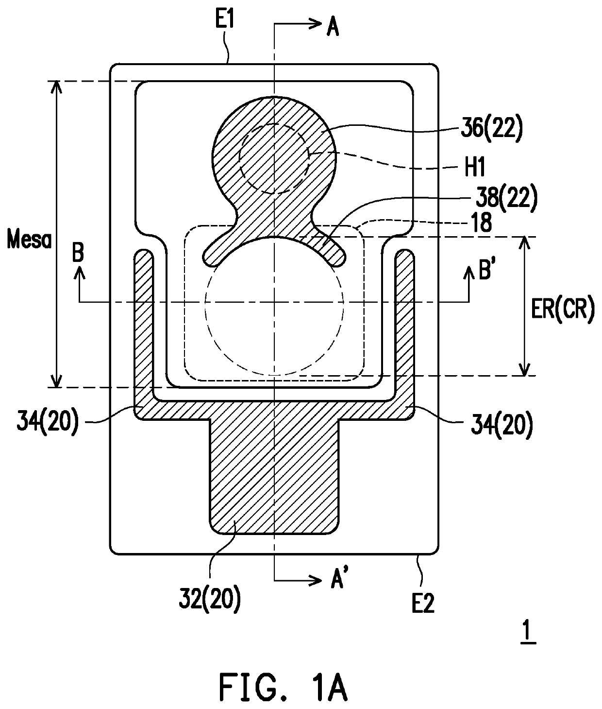
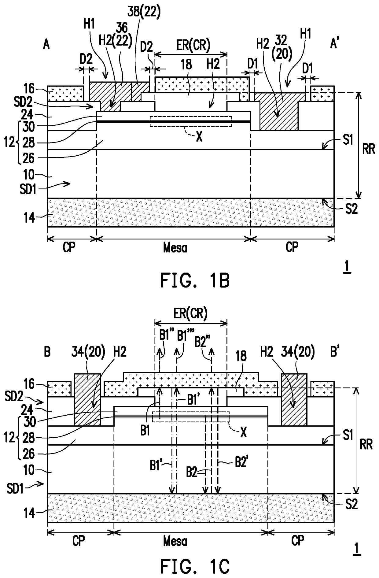
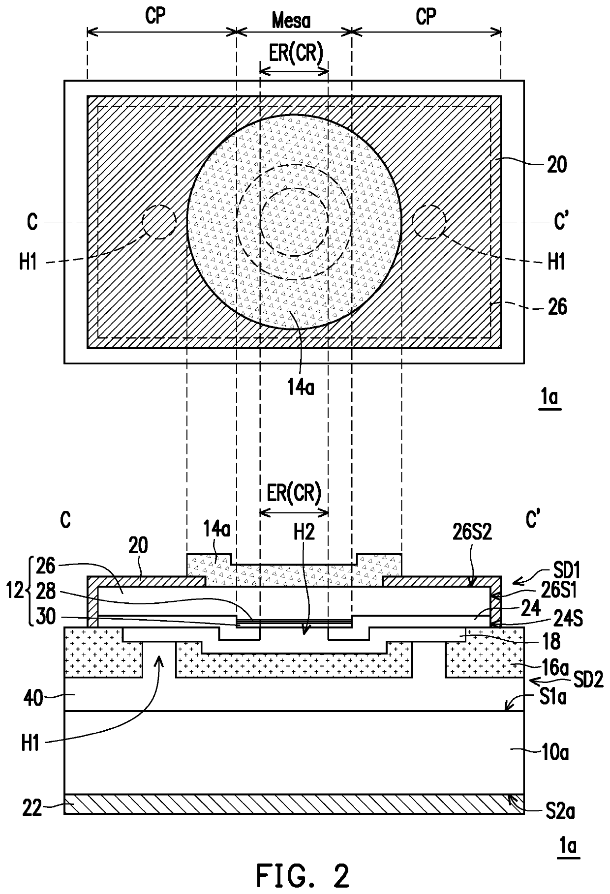
[0028]FIG. 1A is a top view showing a light emitting diode (LED) according to an embodiment of the invention. FIG. 1B and FIG. 1C are respectively schematic cross-sectional views along lines A-A′ and B-B′ in FIG. 1A. For illustrative clarity, a second reflective layer 16 is omitted from FIG. 1A.

[0029]Referring to FIG. 1A through FIG. 1C, in the present embodiment, an LED 1 includes a substrate 10, an epitaxial stacked layer 12, a first reflective layer 14, the second reflective layer 16, a current conducting layer 18, a first electrode 20, a second electrode 22 and a current blocking layer 24. The configuration relationship among the elements will be described in detail below.

[0030]The substrate 10 is, for example, a substrate adaptive for growing the epitaxial stacked layer 12, which may also be referred to as a growth substrate. The substrate 10 has a first and a second surfaces 51 and S2 opposite to each other and is, for example, a sapphire substrate, a gallium nitride (GaN) sub...


PUM


Abstract

A light emitting diode (LED) including an epitaxial stacked layer, first and second reflective layers which are disposed at two sides of the epitaxial stacked layer, a current conducting layer and first and second electrodes and a manufacturing thereof are provided. The epitaxial stacked layer includes a first-type and a second-type semiconductor layers and an active layer. A main light emitting surface with a light transmittance >0% and ≤10% is formed on one of the two reflective layers. The current conducting layer contacts the second-type semiconductor layer. The first electrode is electrically connected to the first-type semiconductor layer. The second electrode is electrically connected to the second-type semiconductor layer via the current conducting layer. A contact scope of the current conducting layer and the second-type semiconductor layer is served as a light-emitting scope overlapping the two layers, but not overlapping the two electrodes.

Description

CROSS-REFERENCE TO RELATED APPLICATION[0001]This application is a continuation-in-part application of and claims the priority benefit of U.S. application Ser. No. 16 / 531,148, filed on Aug. 5, 2019, now pending, which claims the priority benefits of U.S. provisional application Ser. No. 62 / 714,098, filed on Aug. 3, 2018, U.S. provisional application Ser. No. 62 / 816,922, filed on Mar. 12, 2019, and U.S. provisional application Ser. No. 62 / 865,997, filed on Jun. 25, 2019. This application also claims the priority benefit of U.S. provisional application Ser. No. 62 / 775,904, filed on Dec. 6, 2018. The entirety of each of the above-mentioned patent applications is hereby incorporated by reference herein and made a part of this specification.BACKGROUNDField of the Invention[0002]The invention relates to a light emitting diode (LED) and a manufacturing method thereof and more particularly, to a resonant cavity light emitting diode (RCLED) and a manufacturing method thereof.Description of Re...

Claims


Application Information

Patent Timeline
IPC IPC(8): H01L33/46H01L33/00H01L33/14H01L33/38
CPCH01L2933/0025H01L33/007H01L33/465H01L33/145H01L2933/0016H01L33/385H01L33/382H01L33/0093H01L33/38H01L33/14
Inventor HUANG, YI-RUKANG, KAI-SHUNCHUANG, TUNG-LINKUO, YU-CHENLAN, YAN-TINGSHEN, CHIH-MINGHUANG, JING-EN
Owner GENESIS PHOTONICS
Why Eureka
Try Eureka