Unlock instant, AI-driven research and patent intelligence for your innovation.

Apparatus and method for combining analog neural net with FPGA routing in a monolithic integrated circuit

Active Publication Date: 2020-07-30
MICROSEMI SOC
View PDF0 Cites 2 Cited by
  • Summary
  • Abstract
  • Description
  • Claims
  • Application Information

AI Technical Summary

Benefits of technology

The patent describes a method of using a neural network to convert analog input values to digital ones. The method involves a series of small circuits that use a neuromorphic process to convert the analog input to a pulse width that represents the voltage. This pulse width is then converted back to a constant voltage using additional circuits. This approach eliminates the need for multiple conversions and reduces errors, while still achieving the desired function with a single applied voltage. Overall, the method simplifies the process of converting analog input to digital, while achieving higher accuracy and speed.

Problems solved by technology

Building a neural network using digital computation is unsatisfactory because it consumes unreasonable amounts of power.
The neural network functions are implemented in the analog domain in each layer, but problems arise in routing the analog voltage levels to the next layer.
Analog computation of neural network functions consumes less power, but routing a variable voltage is difficult as buffering requires the use of operational amplifiers which introduce errors, and consumes both significant die area and static power.
Such routing is currently designed and hardwired into each integrated circuit individually for each application, making it expensive and inflexible.
It is, however, very expensive to convert back and forth between the digital domain and the analog domain.
In addition such conversions slow down a system as well as providing an opportunity to introduce errors into the computations.
One problem with this scheme occurs when the input voltage is at the high end of the 8-bit range and the programmed variable conductance is at the low end of the transfer curve.
Because the low end of the variable conductance transfer curve is non-linear, the accuracy of the matrix vector multiplier unit suffers the most when the input voltage is at the high end of the 8-bit range and the programmed variable conductance is at the low end of the transfer curve.

Method used


Image

  • Apparatus and method for combining analog neural net with FPGA routing in a monolithic integrated circuit
  • Apparatus and method for combining analog neural net with FPGA routing in a monolithic integrated circuit
  • Apparatus and method for combining analog neural net with FPGA routing in a monolithic integrated circuit

Examples


Embodiment Construction

[0024]Persons of ordinary skill in the art will realize that the following description is illustrative only and not in any way limiting. Other embodiments will readily suggest themselves to such skilled persons.

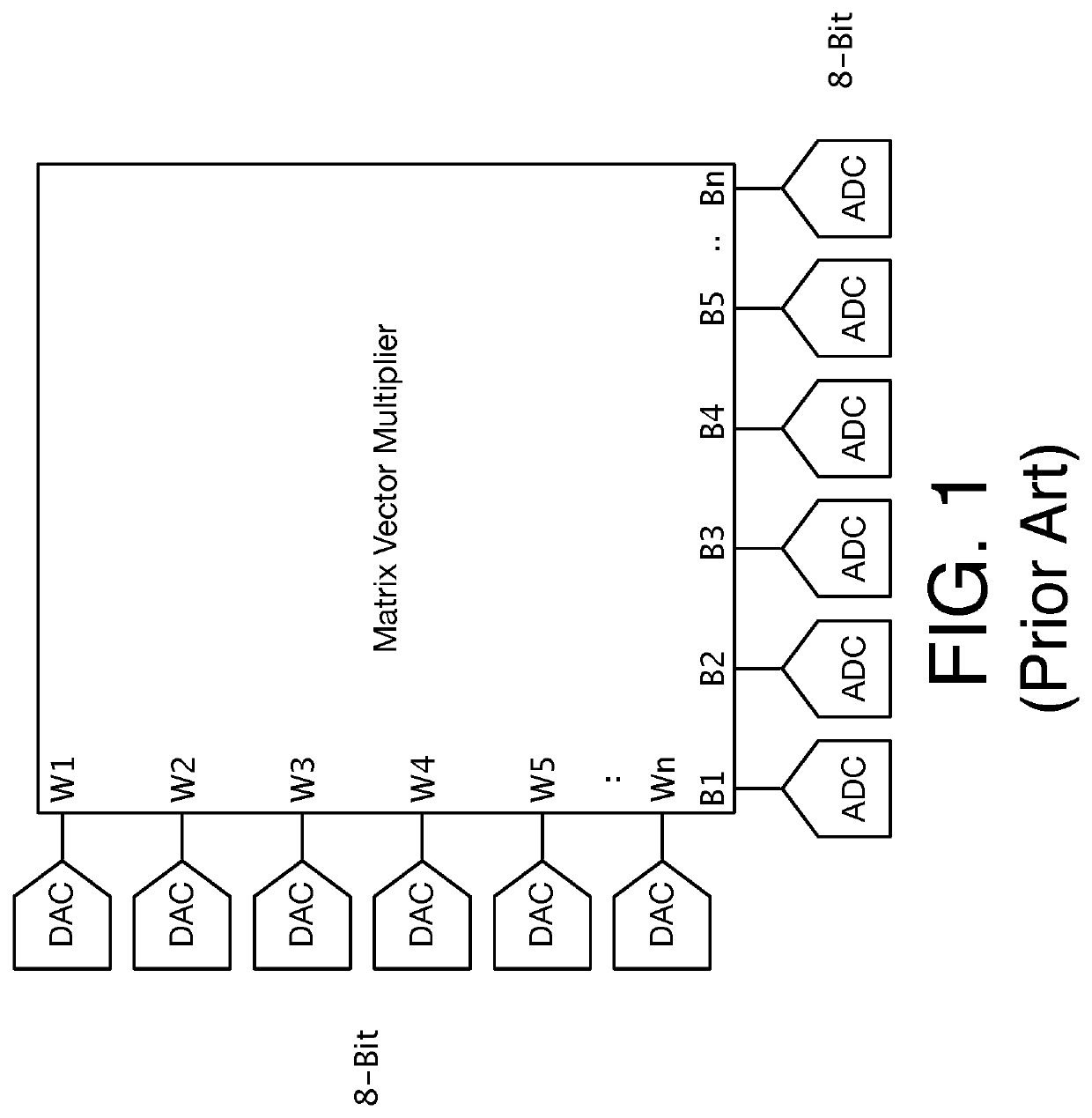
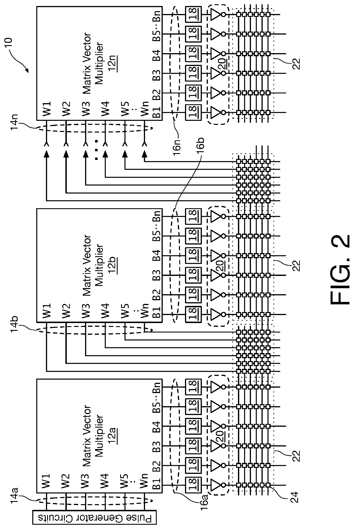
[0025]The present invention uses a switching array similar to that used in FPGAs. Because routing the neural network analog voltages is difficult and expensive, requiring a large number of large power consuming unity gain amplifiers at every switch point, the present invention solves this problem by converting the analog quantities to analog timing pulses which are routed though the switch points.

[0026]Referring first of all to FIG. 2, a block diagram shows a neural network system 10 including a plurality of cascaded matrix vector multipliers 12a, 12b, . . . 12n. Each one of the cascaded matrix vector multipliers 12a, 12b, . . . 12n is a matrix having a plurality of word line (W) inputs 14 identified as W1, W2 . . . Wn and a plurality of bit line outputs 16a, 16b, . . . 16n i...


PUM


Abstract

A user programmable integrated circuit includes a user-programmable routing network including a plurality of interconnect conductors selectively couplable to one another by user-programmable elements. A plurality of matrix vector multipliers, each have a plurality of word lines, each word line coupled to a different first one of the one of the interconnect conductors of the user-programmable routing network, the word lines forming intersections with a plurality of summing bit lines, a programmable Vt transistor at each intersection having a gate connected to the intersecting word line, a source connected to a fixed potential and a drain connected to the intersecting summing bit line. A charge-to-pulse-width converter circuit is associated with each one of the matrix vector multipliers, each having an input coupled to one of the summing bit lines, and a pulse output coupled to a different second one of the interconnect conductors of the user-programmable routing network.

Description

BACKGROUND[0001]The present invention relates to integrated circuit technology. More particularly, the present invention relates to analog neural networks and to combining analog neural networks with field programmable gate array technology.[0002]Neural networks are built by connecting together several functions including matrix-vector products, rectification (RELU activation function), and a maximum of a set of values (max pooling). An ideal neural network integrated circuit could connect these functions together in a programmable manner.[0003]Building a neural network using digital computation is unsatisfactory because it consumes unreasonable amounts of power. Analog Based Neural Network integrated circuits are efficient at calculating the terms for each layer. The neural network functions are implemented in the analog domain in each layer, but problems arise in routing the analog voltage levels to the next layer. Analog computation of neural network functions consumes less power...

Claims


Application Information

Patent Timeline
IPC IPC(8): G06F17/16H03K19/177G06N3/04
CPCH03K19/17744G06F17/16G06N3/04G06N3/0635G11C16/0408G11C11/54G11C7/1006G11C16/0416G11C16/0466G11C16/10G11C7/04G06N3/065G06G7/161G06G7/22
Inventor MCCOLLUM, JOHN L.GREENE, JONATHAN W.BAKKER, GREGORY WILLIAM
Owner MICROSEMI SOC
Features
  • R&D
  • Intellectual Property
  • Life Sciences
  • Materials
  • Tech Scout
  • Unparalleled Data Quality
  • Higher Quality Content
  • 60% Fewer Hallucinations
Learn More