
Eureka
For R&D, Eureka makes reading and utilizing patents & technical documents easy.
Eureka AIR
Designed for self-driven R&D workflows. Generate viable solutions, solve complex R&D challenges, empower your innovation with AI.

Eureka Materials
Designed for material experts only. Revolutionize your material R&D, from search, analyze, to developing new materials.

TechResearch
Generate reliable direction feasibility study reports for your R&D in just a few steps.

TechSeek
Discover and master advanced knowledge NOW. Basics, ideas, possibilities, all at once.

TechMind
As an expert in R&D Theories, TechMind can generates customized viable solutions instantly.

TechRisk
Analyze your overall solution with one click, know your potential R&D risks in advance.

TechMonitor
Get weekly tech updates, stay abreast of the latest tech innovations and key insights.
Micro light emitting device display apparatus
- Summary
- Abstract
- Description
- Claims
- Application Information
AI Technical Summary
Benefits of technology
Problems solved by technology
Method used
Image

Examples
first embodiment
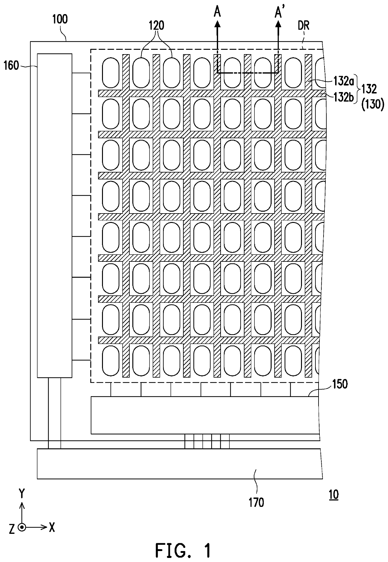
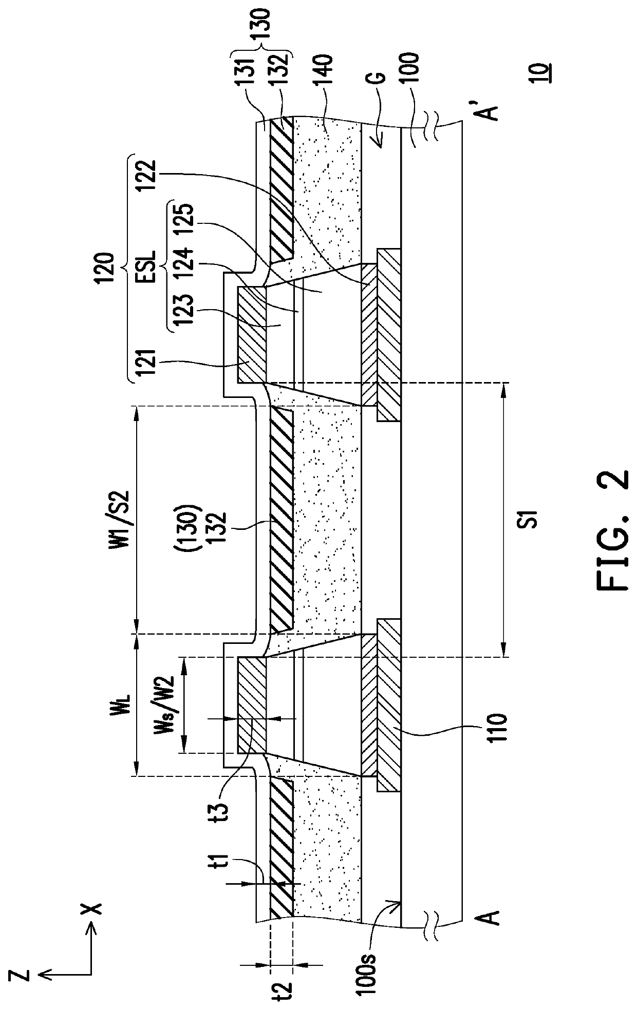
[0040]FIG. 1 is a top view of a micro light emitting device display apparatus of the invention. FIG. 2 is a cross-sectional view of the micro light emitting device display apparatus of FIG. 1. FIG. 2 corresponds to section line A-A′ of FIG. 1. In particular, for the sake of clarity, FIG. 1 omits the illustration of connection pads 110, an isolation layer 140, and a first common electrode layer 131 of FIG. 2.
[0041]Referring to FIG. 1 and FIG. 2, a micro light emitting device display apparatus 10 includes a circuit substrate 100, a plurality of micro light emitting devices 120, and a common electrode 130. The plurality of micro light emitting devices 120 and the common electrode 130 are disposed on the circuit substrate 100, and the common electrode 130 covers the micro light emitting devices 120. More specifically, the circuit substrate 100 has a plurality of connection pads 110 located in a display region DR, and the connection pads 110 are distributed on a surface 100s of the circu...
second embodiment
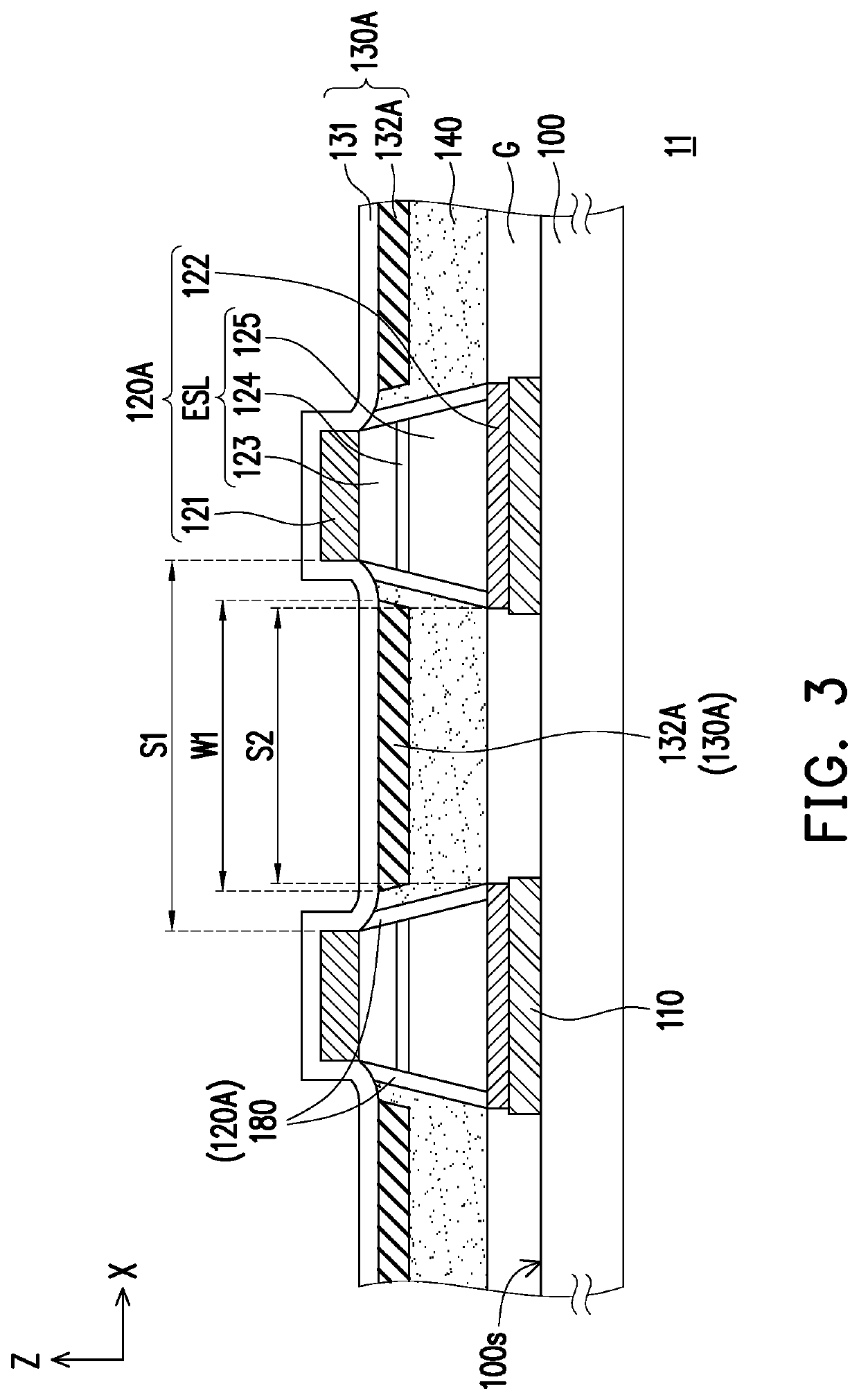
[0059]FIG. 3 is a cross-sectional view of a micro light emitting device display apparatus of the invention. Referring to FIG. 3, the main difference between a micro light emitting device display apparatus 11 of the present embodiment and the micro light emitting device display apparatus 10 of FIG. 2 is that the composition of the micro light emitting devices is different and the size and arrangement relationship of the second common electrode layer are different. Specifically, micro light emitting devices 120A of the micro light emitting device display apparatus 11 may further include an insulating layer 180 disposed between the isolation layer 140 and the epitaxial structure ESL. In the present embodiment, the insulating layer 180 may directly cover the sidewalls of the second-type semiconductor layer 125, the light emitting layer 124, and a portion of the first-type semiconductor layer 123 of the epitaxial structure ESL, but the invention is not limited thereto. Accordingly, a lea...
third embodiment
[0061]FIG. 4 is a cross-sectional view of a micro light emitting device display apparatus of the invention. Referring to FIG. 4, the difference between a micro light emitting device display apparatus 12 of the present embodiment and the micro light emitting device display apparatus 10 of FIG. 2 is that the configuration of the second common electrode layer is different. Specifically, in the present embodiment, there is a first height H1 between a surface 132s of a second common electrode layer 132B of a common electrode 130B connected to the first common electrode layer 131 and the circuit substrate 100, there is a second height H2 between a surface 121s of the first-type electrode 121 connected to the first common electrode layer 131 and the circuit substrate 100, and an isolation layer 140A may be protruded from between the plurality of first-type electrodes 121 of the plurality of micro light emitting devices 120. The first height H1 of the second common electrode layer 132B is g...
PUM
 Abstract
Description
Claims
Application Information
 - R&D Engineer
- R&D Manager
- IP Professional
- Industry Leading Data Capabilities
- Powerful AI technology
- Patent DNA Extraction
Browse by: Latest US Patents, China's latest patents, Technical Efficacy Thesaurus, Application Domain, Technology Topic, Popular Technical Reports.
© 2024 PatSnap. All rights reserved.Legal|Privacy policy|Modern Slavery Act Transparency Statement|Sitemap|About US| Contact US: help@patsnap.com